Quantcast
Channel: LEKULE
Viewing all 1099 articles
Browse latest View live

Concealment Confidence - Taurus 856 .38 Special Revolver

$
0
0
Concealment Confidence - Taurus 856 .38 Special Revolver
The Taurus 856 .38 Special Revolver is definitely an affordable personal protection option worth considering.
Photos by Mike Anschuetz


If you're in the market for a small, concealable, self-defense arm that's as easy on recoil as it is the bank account, it may be time to take a walk on the cylinder side of things and explore the Taurus UL 856 revolver.
Yes, a revolver. In a world saturated with compact semiautomatic pistols, the revolver hasn't been getting the love of many first-time shooters and concealed-carry card holders as it used to. But the .38 caliber that was popular at the turn of the 20th century can still be a viable option for folks looking for operational simplicity and dependability with enough persuasion to stop a threat.
Taurus-856-.38-Special-Revolver-Cylinder
The UL 856, by Taurus, is a six-shot, 2-inch barreled .38 Special that is just over 6.5 inches long and 1.41 inches wide.
The UL 856, by Taurus, is a six-shot, 2-inch barreled .38 Special that is just over 6.5 inches long and 1.41 inches wide. Before you think that seems to be a bit large for a concealed-carry gun, given today's micro semiauto's, the 856 is shorter than a lot of pistols that are considered concealable compacts. This includes the popular Smith & Wesson M&P9 M2.0 and SIG Sauer P320. (The UL 856 actually matches the P320 Compact in width.)

Also, don't think the .38 Special chambering is a detriment. Ammunition today is top notch with loads featuring a wide choice of bullet weights ranging from Hornady's 90-grain Critical Defense loads up to 158-grain round-nose thumpers in Remington's Performance Wheel Gun offering. There are also training loads from Winchester to hone your skills.

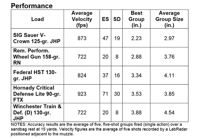
Sure, velocities don't match the 9mms, but even at the velocities I was recording from the Taurus – an average of 923 feet per second (fps) for the 90-grain Hornadys and 722 fps for heavier Remington 158s – they're moving plenty fast. Couple that with the attention to bullet design the ammo gurus are giving them, penetration and expansion isn't a problem at the ranges a snubby would best be utilized.
Taurus-856-.38-Special-Revolver-Hammer
Engaging targets at that distance with the gun's long double-action (DA) pull proved a bit more challenging given the gun's serrated front sight and grooved top strap acting as the rear sight.
At 15 yards, the extreme of what some defense experts claim as the effective range for any defense gun, the 856 proved it had accuracy potential tallying an average of 2.97 inches in single-action (SA) using SIG Sauer's V-Crown 125-grain JHPs. Keep in mind that was from a sandbag rest and the hammer cocked back, which turned the trigger into a buttery-smooth – and crisp – 4 pounder. A far cry from the 10-pound, double-action pull.

Engaging targets at that distance with the gun's long double-action (DA) pull proved a bit more challenging given the gun's serrated front sight and grooved top strap acting as the rear sight. But with a little white out on the front sight and on top of the lands at the rear of the groove, I was able to group six shots with a variety of ammo inside plate-sized targets at 7 yards after some practice adjusting to the DA trigger.
Taurus-856-.38-Special-Revolver-Grip
Taurus compensates for the size of its grip by providing a nicely textured soft rubber grip with finger swells.
Not unlike the 856's semiauto competitors, the grip on the revolver is on the small side. Even with my small hands, I found my pinkie folded under the grip. But this turned out not to be an issue. Taurus compensates for the size of its grip by providing a nicely textured soft rubber grip with finger swells. This provided ample gripping confidence during off-hand drills with my pinkie finger turned into a stabilizer nuzzled up to the soft bottom of the grip.

Firing the gun from a variety of two-hand stances and then one handed, the gun will get the job done hitting torso-sized targets close in. Carrying the 22-ounce, all-steel gun in both a Freedom inside-the-waistband (IWB) holster and in an outside-the-waistband (OWB) Snapslide holster from CrossBreed for a number of days didn't feel much different than carrying a compact semiauto. The gun's curved grip and the holsters' designs that hugged the body helped prevent printing below an untucked shirt or jacket.
Taurus-856-.38-Special-Revolver-Trigger
The heavy DA trigger pull can be considered an additional safety feature by some folks.
The rubber grips make drawing confident and sure with the little finger swell on the right side of the grip telling you if your trigger finger off the trigger or in position with the trigger. And that heavy DA trigger pull can be considered an additional safety feature by some folks.

While there's no arguing the 856's six-shot capacity is less than many compact 9mms (although a few only carry seven shots), I believe the 856 could compensate for the lack of firepower with better accuracy thanks to technology. Adding a laser grip such as Crimson Trace's LG-385 would significantly improve the on-target effectiveness of the gun at ranges out to 15 or 20 yards and make the gun easier to shoot well in reduced-light conditions.
Taurus-856-.38-Special-Revolver-Sight
If I was to have one in a night stand, I'd definitely want a laser grip on the gun.
If I was to have one in a night stand, I'd definitely want a laser grip on the gun. Its iron sights are hard enough to aim during the day, and at night they would be useless. A laser would give aim and shoot capability.

After practicing with the revolver, I grew to appreciate the confident availability of a new round rotating in place without concern for a feeding or extraction malfunction. Besides concealed carry, I could see a gun like this in a tackle box or in a glove compartment of a vehicle.

With a manufacturer's suggested retail price of $329, I do believe one could cross the counter at a dealer for under $300. Definitely an affordable personal protection option worth considering.
Taurus-856-.38-Special-Revolver-Performance
Specifications
Taurus UL 856
Type: DA/SA Revolver
Cartridge: .38 Special
Capacity: 6 rds.
Overall Length: 6.5 in.
Height: 4.8 in.
Width: 1.41 in.
Barrel Length: 2 in.
Weight: 22 oz.
Material: Steel
Grip: Soft rubber
Trigger: 10 lbs. (DA), 4 lbs. (SA)
Safety: Transfer bar
Finish: Matte black
Sights: Fixed serrated-ramp front, fixed groove rear
MSRP: $329
Manufacturer: Taurus
800-327-3776,

taurususa.com

How Team Wendy Is Changing the Science Behind Protective Helmets

$
0
0
The story behind Team Wendy and how its high-tech helmets are keeping military and law enforcement protected from traumatic brain injury.


The phrase “game changer” gets overused in a lot of mediums. However, when it comes to Team Wendy’s focus on preventing traumatic brain injury, its helmets truly are game changers.

Jump School

When I went through the U.S. Army jump school in the 1980s, we were issued classic two-part steel pot helmets. My roster number, C174, was stenciled across the front, and my copy looked like it had been in service since the American Revolution. I walked to the PX and bought myself a new leather sweatband because the version already in my high-mileage lid likely harbored disease.

These were the same basic armored helmets that had carried our forefathers through World War II. The liner was made from some kind of synthetic material and was both lightweight and removable. The heavy bit was pressed from manganese steel and could be suspended over a fire as a cooking pot in a pinch.

I thought we were high speed because, unlike the same helmet I wore when I was not jumping out of airplanes, this one had a stiff foam pad sticking out the back to nominally protect the nape of the neck. On our first jump, one unfortunate member of my stick had his helmet ripped away as soon as he leapt into the prop wash. Thankfully no one was killed when the dislodged lid subsequently bounced into the drop zone below. With kit like that, it’s a wonder any of us survived.

The Processor

The human brain is the most complex contrivance in the known universe. The CPU on the latest F-35 multirole fighter plane pales in comparison to the phenomenal computational capabilities of the fingertip-sized mind of the squirrel that raids your wife’s bird feeder. Not only can we do precious little to fix a brain when it gets broken, but we don’t really even understand it terribly well.

Humans have the largest brains relative to their body size of any known animal. A typical human brain weighs about 3.33 pounds and makes up around two percent of a typical person’s body weight. A human brain sports around 86 billion neurons that form via their axons and dendrites literally trillions of connections (that’s 12 zeroes). To claim that we can even begin to comprehend the engineering elegance behind this most remarkable of computers is the apex of farce.

To maximize the number of neurons per unit volume, the brain is designed with gyri and sulci; these are the variegated wiggles and valleys that characterize the unique surface of the brains of complex organisms. Intelligent animals like chimpanzees and dolphins have lots of these hills and valleys. Less intelligent creatures like mice, Socialists and gun-control advocates have smooth brains.

For all of its literally breathtaking complexity, the human brain, being comprised predominantly of fat, remains remarkably fragile. The skull is a superbly designed armored carapace that helps protect this delicate instrument from variegated mischief. However, as we humans push the boundaries of exploration, sports and combat, we find ourselves in desperate need of yet better protection for this most sensitive of mechanisms.

The Problem

Now well into the Information Age, science has changed most every aspect of armed combat. The scourge of the IED, combined with the unique rigors of a protracted unconventional war across an asymmetrical battlefield, conspires to offer new and unique challenges for our men and women serving downrange. These travails have brought the power of science to bear on the thorny problem of protecting the remarkable computer that sits astride your shoulders from the sundry malice specifically contrived to destroy it.

Where previously we just dropped a bit of manganese steel atop our otherwise unadorned domes and called it good, nowadays a great deal of thought and treasure has gone into maximizing the brain’s defenses against shock, pressure and blunt-force trauma.

The challenge is timeless and the stakes astronomical. While lots of folks have tackled this prickly problem, none have pushed the boundaries so far as Team Wendy. To understand the passion Team Wendy has for mitigating brain injuries, you need to know the remarkable narrative that drives its zeal.

The Backstory on Team Wendy

Team Wendy draws its name from a young lady named Wendy Moore. Her father, Dan, tragically lost his daughter to a traumatic brain injury stemming from a skiing accident in the 1990s.
Where many of us dads would have allowed an immeasurable tragedy of this sort to destroy us, Dan translated his loss into a superhuman drive to protect others from a similar fate. That singular event drove Dan Moore to found Team Wendy with the mission of producing the finest protective headgear the world has ever seen.

Evolution

The company began in 1997 with ski helmets. As the science of helmet design evolved, Team Wendy delved into high-tech helmets for law enforcement, military, and search and rescue applications.
Nowadays, Team Wendy’s mandate is to research, develop, design and deliver the most innovative, protective and impact-mitigating products and technologies in the world while simultaneously researching the causes and prevention of traumatic brain injury (TBI).

Out of one father’s incalculable loss came new technologies that have ultimately saved countless lives already.

Zorbium

The company produces helmets for a remarkably long list of applications, but those helmets share a common beating heart. Team Wendy’s most notable developmental accomplishment to date is a patented impact-mitigating foam called Zorbium. First developed for ski and multisport helmets, this material has found a home in tactical and search and rescue helmets as well.

Zorbium provides a significant increase in blunt impact protection and has been incorporated into the standard-issue helmet pads of both the U.S. Army and Marine Corps since 2005. Zorbium dropped the peak “G” threshold for padded combat helmets by 50 percent over previous designs. That simply means it does a much better job of protecting your head.

Team Wendy does its own in-house development of material technologies, as well as morphological design. New helmets begin as brainstorming concepts before advancing through refinement, testing and ultimately practical validation. Team Wendy’s unique grasp of material development, combined with end-user requirements, has produced some of its most successful products.

Team Wendy prides itself on being large enough to meet the demands of government users while remaining sufficiently agile to respond to the rapidly evolving needs of its customers. The company’s production processes include foam production, radio frequency sealing, fabric cutting, sewing and final helmet assembly. The folks at Team Wendy fully appreciate the holy nature of their mission; subsequently, they build world-class quality into every helmet they produce.

GO Gear

Team Wendy’s flagship product is the EXFIL line of helmets. Available in four primary configurations, all EXFIL helmets are designed to be comfortable, lightweight and protective. The specific models in this line are the EXFIL Carbon, the EXFIL LTP (Lightweight Tactical Polymer), the EXFIL SAR (Search and Rescue) and the EXFIL Ballistic.

EXFIL Features

The entire EXFIL line shares a common array of features. The primary differentiators between the basic configurations are the performance specifications. All helmets in the line conform to the military blunt-impact standards. The Carbon, LTP and SAR helmets are all non-ballistic, meaning they are not designed to resist bullets and shrapnel. The LTP meets the EN 1385 standard for whitewater helmets. The SAR meets commonly accepted mountaineering and industrial standards. The EXFIL Ballistic meets accepted ballistic benchmarks. As you can imagine, the more rugged the material, the heavier the helmet.

The EXFIL Ballistic helmet is available with a robust ballistic-resistant shell. The lightweight, non-ballistic EXFIL Carbon synthetic carbon- fiber helmet is offered for modestly violent applications. The LTP bump shell is rated against mild impacts, as is the dedicated SAR variant. In these four configurations, the common EXFIL design offers a range of protection from high-velocity bullets down to the sorts of bumps and scrapes you might acquire during basic adventurous activities. By utilizing a common suspension and retention system along with a communal family of external accessories, a singular helmet design is optimizable for most any conceivable application.

EXFIL helmets employ an innovative boltless CAM FIT retention system that is easily adjustable and maximizes user comfort. This unique system conforms to various head shapes to ensure stability and security. This retention system also allows one-handed adjustment for a proper fit. A Boa closure system keeps everything snug.

Liners

Moveable comfort pads optimize the Zorbium foam liner. These pads are available in two thicknesses to conform to varying anatomy. This liner accommodates an overhead communications headband via a removable center pad while still protecting against violent impacts. This same system has been combat proven in the standard Advanced Combat Helmet (ACH) Zorbium Action Pad (ZAP) system used in U.S. military helmets.

The U.S. Army Natick Soldier RD&E Center HEaDS-UP Program originally designed an alternative thermoplastic urethane (TPU) Hybrid liner. These TPU liners are optimized for impact protection. The resulting design maximizes airflow and ventilation by creating a standoff area between the operator’s head and the helmet shell. This particular liner option is only available on the EXFIL Carbon. Team Wendy recently updated the design to be identical to the REVOLVE liner system.

Mounting

The exterior of the EXFIL Ballistic, Carbon and LTP shells sports a Rail 2.0 mounting system, as well as T-slots for incorporating accessories. There is also a pair of Magpul MOE Picatinny-style rails for any imaginable accessory bling. A lanyard-compatible Wilcox shroud accommodates night-vision systems.

On the Horizon

Team Wendy also has some exciting new products in the pipeline. These include an armored mandible attachment that affixes to the helmet’s organic rails. This accessory will provide ballistic protection for the face and jaw as well as applique armor that provides protection against 7.62x39mm M43 rifle rounds. The company will also soon be offering side armor components that provide as much coverage as the current ACH combat helmet. A rail-mounted ballistic visor is in the works as well.

The Passion

The world has indeed come a long way since I first stood quivering in the door of a thundering C-130 underneath my WWII-era manganese steel combat helmet so many years ago. Meanwhile, traumatic brain injury continues to take a toll on our brave warriors serving downrange. However, new mine-resistant, blast-resistant vehicles combined with such high-tech stuff as Zorbium and the Team Wendy EXFIL helmets serves to mitigate its effects.


This story is from the spring 2018 issue of Ballistic Magazine. Grab your copy at OutdoorGroupStore.com.

Bravo Concealment BCA 3.0 OWB

$
0
0
With new polymer for improved strength and an adjustable retention system, the Bravo Concealment BCA 3.0 OWB hoster adds comfort and flair to EDC.


Concealment holsters are extremely personal, which is why there are so many different designs available. Additionally, sometimes companies improve on their designs, which is what happened with the Bravo Concealment BCA 3.0 OWB holster.

Bravo designed the BCA originally from Kydex to comfortably snug the body for concealment. The company chose Kydex for its durability. The holster also featured the ability to be converted to IWB, makeing the holster ideal for multiple uses. Additionally, the BCA allowed use of threaded barrels, tall sights and even RMR sights. Bravo kept these great features, but added some improvements to the BCA 3.0 by making the holster “personal.”

To start, Bravo used a diversified polymer plastic known for its balance between rigidity, impact strength and hardness. Now the holster better protects firearms, whether re-holstering constantly at the range or carrying on a daily basis. Additionally, Bravo added a solid-locking adjustable retention system. This allows users to customize retention from medium light to very heavy, which is an excellent feature. The company also reduced the footprint by eliminating material from it’s bottom corners to make it smaller and lighter. This makes the holster even more comfortable to use.

Currently, the BCA 3.0 is available for Glock handguns, even the Gen5 Glocks. However, those who prefer earlier generations are out of luck. The BCA 3.0 does not accommodate Gen1 or Gen2 Glock handguns. However, shooters who own a model that fits, should consider adding some flair to their everyday carry rig.

Bravo Concealment BCA 3.0 OWB Holster

  • Threaded Barrel clearance
  • Tall Sights clearance up to .355 (In)
  • Red Dot Sight (RMR) cut-out
  • Adjustable Retention
  • 1.50″ Standard Belt Loops
  • Color: Black
  • Solid locking adjustable retention (NEW)
  • Minimalist Design for even more all day comfort (NEW)
  • Polymer plastic provides supreme rigidity and impact strength assuring protection of your firearm. (NEW
  • Designed for outside the waistband carry, but can easily be converted to inside the waistband by swapping out the belt loops with our IWB belt clips.
  • 10° cant enhances concealment under loose garments.
  • Robust 1.50” or 1.75” injection molded belt loops prevent breakage even under rigorous use.
  • Belt loops can be replaced with Belt Clips for inside the waistband carry.
  • The BCA creates adequate room for a positive grip thus enabling a smooth draw with solid weapon retention.
  • All edges on holster are rounded for comfort.
  • All holsters are curved to fit the contours of your body.
  • MSRP: $57.99

For more information about the Bravo Concealment BCA 3.0 OWB holster, please visit bravoconcealment.com, or watch the video below.

Does the IoT Need Oversight? UK Introduces “Code of Practice” of Cybersecurity for IoT Developers

$
0
0
The British government recently released a "Code of Practice" for IoT device developers to responsibly design secure devices. Is this list of best practices a precursor to regulation? Should it be?
It is estimated that there are over 23 billion IoT devices currently connected worldwide and this number is expected to increase to 75 billion by 2025. Securing these devices has become a global conversation.

Individual companies are expected to have security in mind when they design, manufacture, and sell their devices. But, with more and more IoT devices coming into operation, governments are looking at becoming involved.

Understanding Security Threats for IoT Devices

While IoT devices are often simple and unable to process large amounts of data (especially when compared to desktop PCs and tablets), they do possess one ability that requires very little processing power: they can send messages across the internet and often record data about their environment. One IoT device on its own cannot do much—but when combined with a thousand other devices then suddenly a DoS (Denial of Service) attack becomes possible.

In order for an authorized party to gain access to an IoT device, they first need to hack the device either physically or remotely.

Physical hacks involve reverse engineering the circuitry and trying to find unsecured bus lines or debug ports that allow the hacker to gain entry into the firmware. From there, potentially sensitive information such as usernames and passwords can be found, as well as certificates and even security flaws in the system. Remote hacking involves trying to hijack the IoT device remotely (i.e., from anywhere in the world) whereby a hacker can attempt to login to the device and update the firmware with one that contains malware (to allow control of the device).

Remote hacking using techniques such as brute force for login details can be applied to weak passwords but more times than not hacking can be done in as few as 60 username/password combinations.

Surely such malware must be incredibly well engineered if hacks can be done in under 60 combinations? Does the malware use a special byte-code that can unlock machinery? The true answer is shocking and has governments seriously concerned to the point where they are considering regulating the industry.


Security Ignorance: A Key Failing for Cybersecurity

Many products on the market take advantage of pre-made packages such as Linux which can be made to run on small ARM microcontrollers. While this provides a useful platform to build applications on, it also comes with some serious security risks.

Unfortunately, most (if not all) operating systems come with default username and passwords (such as “admin” and “password”) and, if the user does not change these, then almost any hacker can gain entry in seconds. Such systems may also have legacy services running (such as telnet) that give attackers entry points. When combined with default usernames, the result is a device that can easily be accessed remotely.

This is what happened with the Mirai infection, which would scan the internet for specific IP address of IoT devices and then attempt to login using telnet and 60 common usernames/passwords. Once in, Mirai then installs its own firmware which turns the IoT device into a bot and adds it to a collective which can be used to launch DoS attacks.

Mirai was not able to spread easily because of hardware flaws or unforeseen security holes. The severity of this particular attack was due to either engineers from multiple companies not having a basic understanding of security, not appreciating the potential dangers of IoT devices as bots, not understanding the Linux system—or just because of general ignorance.

While these issues are certainly important from an industry standpoint, they're also crucial from an infrastructure standpoint as the IoT integrates into the very systems that run modern life.

Hacking Infrastructure, Today and Tomorrow

Hacks of payment systems via streaming platforms (Spotify, Sony, etc.) have spurred various reactions from regulatory bodies. But while information security is a concern, there is considerably more apprehension regarding public services such as traffic control, power distribution, and water.
In the past, such services have had electronic equipment but they were not accessible via the internet and the only way such services could be targeted was through physical intervention. Now, with the rise of the internet, cyber attacks can be potentially launched from remote locations to disrupt such services.

As it turns out, infrastructure attacks are already happening—and have been for years. Ukraine has reportedly sustained years of attacks to their infrastructure via cyber attacks, sometimes leaving thousands without electricity.

Some examples are less dire, such as when hackers activated the tornado siren system in Dallas, Texas last year. Activating the system when it isn't needed does have negative repercussions, but the implication that hackers could disable the system when it is needed is more unsettling.
Concern for the security of high-tech systems is growing by the day. Ballot processing has been an area of contention as vulnerabilities in electronic voting machines could have far-reaching consequences on the global scale.

The long-heralded smart city concept also represents a veritable quagmire of vulnerabilities. IoT sensor systems embedded throughout cities have promised more efficient utilities and better safety for years. They may also one day soon become the lynchpin for the autonomous vehicle industry, guiding with self-driving cars through V2X communication.

With this much of our technological future at stake, preventative action against cyber attacks is paramount. But who defines what cybersecurity best practices are?

Cybersecurity Oversight and Best Practices

Security is clearly a point of discussion for governments all over the world. On one hand, oversight infrastructure must first be created in order for action to even be possible. The US Congress, for example, proposed the Cybersecurity and Infrastructure Security Agency Act of 2018 (or CISA) in the US Congress.

On the other hand, authorities can issue best practices. The British Government recently launched its “Code of Practice”, which is a guideline of suggestions for engineers who design IoT projects. Suggestions include giving each device unique usernames and passwords, not using unencrypted message protocols (HTTPS over HTTP), providing certificates for each IoT device, taking advantage of specialized hardware that can store keys securely, and keeping software up-to-date.

Currently, these are only suggestions and not the law, which means engineers are still free to use default passwords and HTTP for communication. However, some security experts, such as Bruce Schneier, believe that intervention is necessary—even to the point of slowing innovation in order to give security time to catch up. Others question whether it's necessary to make basic security practices mandatory.

Such ideas could arguably make it harder for businesses to sell products due to red tape and the possible requirements of submitting technical documents to a security board. By the same token, some believe that these measures could prevent damage to critical services and protect economies.


As an engineer, I often dislike regulation which may make it harder to get products on the market with pointless paperwork and bureaucracy. On the issue of security, however, I am in favor of regulation of some kind. Banks, for example, have to follow strict requirements to ensure that accounts are secure. Does it make sense for hardware and software developers to follow some standard? This could involve microcontrollers using unsecured buses to communicate to memory modules that store passwords, using software that has default passwords, or using plaintext messaging schemes over the internet.

What are your reactions to the prospect of regulations placed on security for device design?

How Design Kits Simplify IoT’s Last Mile to the Cloud

$
0
0
A sneak peek of two IoT platforms allows developers to save time and cost while they streamline connectivity to the cloud services.

A new crop of the Internet of Things (IoT) development kits is simplifying design work while streamlining the last mile that links embedded systems to the cloud. This article will present two case studies that allow IoT designers to quickly implement their ideas with a combination of modular hardware and software solutions.

PI Development Hardware

First, take UrsaLeo kit from RS Components (RS), which comes with pre-registered access to the Google Cloud. The IoT kit allows developers to configure their own dashboards and charts, so they can set event-based text or e-mail alerts and run Google analytics.

The apps and APIs in the UL-NXP1S2R2 kit help IoT designers manage sensors, run diagnostics, and share information with enterprise software or third-party tools. RS Components is targeting this kit at the IoT sensing designs employed in automotive diagnostics, healthcare, and general data monitoring applications.


The UrsaLeo sensor kit allows developers to collect and analyze data on a dashboard within minutes. Image courtesy of RS Components.

The IoT platform is based on a Silicon Labs Thunderboard™ 2 sensor module which is ready to connect to the Google Cloud services. The module contains sensors for temperature, humidity, UV, ambient light, barometric pressure, indoor air quality, and gas detection. It also features a digital microphone, a 6-axis inertial sensor, and a Hall sensor.

The UrsaLeo kit also features the EFR32™ Mighty Gecko multi-protocol 2.4 GHz radio from Silicon Labs. It supports Thread, ZigBee®, and Bluetooth® Low Energy (BLE) as well as proprietary short-range wireless protocols. The kit also offers a ceramic antenna, four high-brightness LEDs, and a coin cell or external battery pack.

Portable Software Agent

A portable software agent from Ayla Networks is another use case showing how IoT platforms are simplifying connectivity to the cloud services. It allows IoT developers to select any cellular or Wi-Fi module and have it connected to the Ayla IoT cloud without a lengthy certification process.
Generally, for a specific connectivity chip or module, IoT designers have to build software and then have it certified. That inevitably results in time and cost overhead. What Ayla has done here is bypasses this need to generate source code to port software on a specific connectivity module.

A view of how a communication module pre-loaded with a portable software agent facilitates connectivity to the cloud. Image courtesy of Ayla Networks.

So IoT developers can pick any connectivity hardware and use Ayla's portable agent software to connect to the cloud service. The portable agent comprises of source code, reference implementation, a porting guide, and a test suite for both cellular and Wi-Fi solutions. Ayla also recommends development partners to perform porting work for IoT designers that don't have the in-house firmware team.


The development kits explained in this article are a testament of how IoT platforms can play a vital role in quickly adding application enablement capabilities to the connected embedded systems—and how IoT developers can focus on their business priorities instead of getting stuck into the IoT's connectivity labyrinth.


What other IoT kits have caught your eye recently? Let us know in the comments below.

Is IoT Getting Out of Control with Smart Ovens?

$
0
0
We have “smart” everything these days, from watches to door locks, the IoT has converted mundane everyday items into connected devices.

So it seems natural that one of the most recent areas to enjoy the touch of IoT is that of the counter top oven. Sure, ovens aren’t the sexiest things ever but you would be surprised about the level of technology inside of them! One such device is the Tovala Smart Oven that recently reached their funding goal on Kickstarter. The Tovala allows you to connect it to your smartphone in order to change cooking settings. It will not only cook your food through traditional baking and broiling, but it can even steam your food. Time to leave the Hot Pockets at the store!  


What’s really tasty is the technology that lies within the Tovala. This allows it to not only connect to your phone but also recognize special food packages for automatic cooking. First things first, regardless of whether you are making a home prepared meal or one of Tovala’s pre-made meals, it automatically controls the cooking chamber. It can even bounce between various cooking modes for optimal cooking via special algorithms. Tovala can even scan meals made by them and configure the settings automatically. Wireless connectivity is brought to you by the Particle PØ Wi-Fi module and the Broadcom BCM43362 Wi-Fi chip. If you’re sick of microwaved food, you can head over to their Kickstarter and pick one up for $199.

If you can afford a more pricey smart oven, you can even remotely watch your food cook with the June Intelligent Oven. The June Intelligent Oven has a host of features that bring counter top ovens into the 21st century, the most interesting of which is the HD camera. The camera isn’t just a gimmick, though, it allows June to automatically identify what you’re cooking and switch to the appropriate settings. The feet of the device also have load cells so you can use the top of the oven to weigh your food for proper cooking times.


Dominating the façade is an edge to edge glass door with an integrated five-inch touchscreen and metal dial for adjusting settings. You also have the option of using a special app to keep tabs on what’s cooking remotely. At the heart of the June oven beats a quad-core NVIDIA Tegra K1 processor with a 2.3GHz clock rate. Driving that tasty little display is an NVIDIA GPU sporting 192 CUDA cores. In-oven camera views and CUDA cores don’t come cheap, however, with the June ringing in at a hefty $1495. More information on reserving one can be found at their website.

Each oven occupies a different end of the price spectrum, but both strive to simplify our extremely busy lives through integrating the latest technology. These are probably just the beginning of an IoT oven revolution and it will be interesting to see what kind of hardware is packed into the next generation of smart ovens.

We've Been Talking About Self-Driving Car Safety All Wrong

$
0
0


Until a self-driving Uber killed 49-year-old pedestrian Elaine Herzberg in March, autonomous vehicle tech felt like a pure success story. A hot, new space where engineers could shake the world with software, saving lives and banking piles of cash. But after the deadly crash, nagging doubts became questions asked out loud. How exactly do these self-driving things work? How safe are they? And who’s to guarantee that companies building them are being truthful?

Of course, the technology is hard to explain, much less pull off. That’s why employees with the necessary robotics experience are raking in huge paychecks, and also why there are no firm federal rules governing the self-driving car testing on public roads. This fall, the Department of Transportation restated its approach to AVs in updated federal guidelines, which amounts to: We won’t pick technology winners and losers, but we would like companies to submit lengthy brochures on their approaches to safety. Just five developers (Waymo, GM, Ford, Nvidia, and Nuro) have taken the feds up on the offer.

Into this vacuum has stepped another public-facing metric, one that’s easy to understand: how many miles the robots have driven. For the past few years, Waymo has regularly trumpeted significant odometer roll-overs, most recently hitting its 10 millionth mile on public roads. It’s done another 7 billion in simulation, where virtual car systems are run over and over again through situations captured on real streets, and slightly varied iterations of those situations (that’s called fuzzing). Internal Uber documents uncovered by the New York Times suggest the ride-hailing company tracked its own self-driving efforts via miles traveled. It’s not just companies, either: Media outlets (like this one!) have used miles tested as a stand-in for AV dominance.

If practice makes perfect, the more practice your robot has, the closer it must be to perfect, right? Nope.

“Miles traveled standing alone is not a particularly insightful measure if you don't understand what the context of those miles were,” says Noah Zych, the head of system safety at the Uber Advanced Technologies Group. “You need to know, ‘What situations was the vehicle encountering? What were the situations that the vehicle was expected to be able to handle? What was the objective of the testing in those areas? Was it to collect data? Was it to prove that the system was able to handle those scenarios? Or was it to just run a number up?”

Think about a driver's license exam: You don't just drive around for a few miles and get a certificate if you don’t crash. The examiner puts you through your paces: left turns across traffic, parallel parking, perfectly executed stop sign halts. And to live up to their promises, AVs have to be much, much better than the humans who pass those tests—and kill more than a million people every year.
Waymo, which has driven more miles than anyone and plans to launch a commercial autonomous ride-hailing service this year, says it agrees. “It’s not just about racking up number of miles, but the quality and challenges presented within those miles that make them valuable,” says spokesperson Liz Markman. She says Waymo also keeps a firm eye on how many miles it’s driving in simulation.

Another safety benchmark used in media coverage and policy discussions of AVs are “disengagements”—that is, when a car comes out of autonomous mode. In California, companies must note and eventually report every instance of disengagement. (They are also required to file an accident report for every crash incident, be it a fender-bender, rear-end, or being slapped by a pedestrian.) Developers say disengagements are an even crappier way to measure safety than checking the odometer.

“If you’re learning, you expect to be disengaging the system,” says Chris Urmson, the CEO of self-driving outfit Aurora, who led Google’s effort for years (before it took on the name Waymo). “Disengagements are inversely correlated with how much you’re learning. During development, they are inversely correlated with progress.” Urmson and others argue California’s reporting requirements actually disincentivize pushing your system to evolve by taking on harder problems. You look better—to the public and public officials parsing those numbers—if you test your cars in situations where it’s less likely to disengage. The easy stuff.

So the way we’re talking about safety for self-driving cars right now is not great. Is there a better way?

Earlier this month, the RAND Corporation, a policy think-tank, released a 91-page report on the concept of safety in AVs. (Uber funded the study. The ride-hailing company and RAND say the report was written and peer-reviewed by company- and tech-neutral researchers.) It details a new sort of framework for the testing, demonstration, and then deployment of AVs, a more rigorous way to prove out safety to regulators and the skeptical public.

The report advocates for more formal separations between those stages, disclosures about how exactly the technology works in specific environments and situations, and a moment of transparency during the demonstration period, as the companies prepare to make money off their labors. And for a new term, called “roadmanship”, a metric that seeks to more fully capture how AVs are playing with other actors on public roads.

And in doing so, the report seeks to be a launch pad for understandable, less opaque language about self-driving cars—language that companies, and regulators, and the public can use to talk, seriously, about the technology's safety as it develops.
The problem, of course, is that autonomous vehicle developers are worried about sharing anything. RAND, which interviewed companies, regulators, and researchers for the report, “had to convince people that we were not going after anything proprietary or highly sensitive,” says Marjory Blumenthal, a RAND policy analyst who led the project. And that’s just to collect information about methods of collecting information! Now imagine getting all those mistrusting players to agree on safety framework that requires them to be much more transparent with each other than they are right now.

But safety advocates argue such a framework is badly needed. “Most people, when they talk about safety, it’s ‘Try not to hit something,’” says Phil Koopman, who studies self-driving car safety as an associate professor at Carnegie Mellon University. “In the software safety world, that’s just basic functionality. Real safety is, ‘Does it really work?’ Safety is about the one kid the software might have missed, not about the 99 it didn’t.” For autonomous vehicles, simply being a robot that drives won’t be enough. They have to prove that they’re better than humans, almost all of the time.

Koopman believes that international standards are needed, the same kind with which aviation software builders have to comply. And he wishes federal regulators would demand more information from self-driving vehicle developers, the way some states do now. Aurora, for example, had to tell Pennsylvania’s Department of Transportation about its safety driver training process before receiving the state’s first official authorization to test its cars on its public roads.

The companies should want to come together on firmer rules, too. Blumenthal says firm and easy to understand safety standards could help the companies in inevitable legal cases, and when they stand in the court of public opinion.

“When you have different paths taken by different developers, it makes it hard,” Blumenthal says. “There's a demand for a common reference point so the public can understand what’s going on.” Safety, it turns out, is good for everyone.

History of the PLC

$
0
0
The PLC or Programmable Logic Controller has revolutionized the automation industry. Today PLCs can be found in everything from factory equipment to vending machines, but prior to New Year’s Day 1968 the programmable controller didn’t even exist. Instead what existed was a unique set of challenges that needed a solution. In order to understand the history of the PLC we must first take some time to understand the problems that existed before programmable controllers.

Before the Programmable Controller

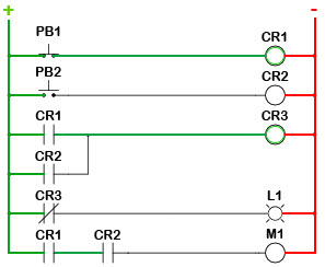
Before the days of the PLC the only way to control machinery was through the use of relays. Relays work by utilizing a coil that, when energized, creates a magnetic force to effectively pull a switch to the ON or OFF position. When the relay is de-energized, the switch releases and returns the device to its standard ON or OFF position. So, for example, if I wanted to control whether a motor was ON or OFF, I could attach a relay between the power source and the motor. Then I could control when the motor is getting power by either energizing or de-energizing the relay. Without power, of course, the motor would not run, thus I am controlling the motor. This type of relay is known as a power relay. There could be several motors in one factory that need to be controlled, so what do you do? You add lots of power relays. So factories started to amass electrical cabinets full of power relays. But wait, what switches the coils in the power relays ON and OFF before the power relay turns the motor ON, and what if I want to control that? What do you do? More relays. These relays are known as control relays because they control the relays that control the switch that turns the motor ON and OFF. I could keep going, but I think you get the picture of how machines were controlled pre-PLC, and, more importantly, I think you start to see some of the problems with this system of electromechanical control via relays.

History of the PLC
Courtesy of Signalhead via Wikimedia Commons

The Problem with Relays

Think about modern factories, and how many motors and ON/OFF power switches you would need to control just one machine. Then add on all the control relays you need and what you get is… Yes, machine control, but you also get a logistical nightmare. All these relays had to be hardwired in a very specific order for the machine to work properly, and heaven forbid if one relay would have an issue, the system as a whole would not work. Troubleshooting would take hours, and because coils would fail and contacts would wear out, there was need for lots of troubleshooting. These machines had to follow a strict maintenance schedule and they took up a lot of space. Then what if you wanted to change something? You would basically have to redo the entire system. It soon became clear that there were problems installing and maintaining these large relay control systems.

Let’s hear from a controls designer in the thick of things in the early ‘70s –
“Upon graduating from technical college in 1970, I began working as a controls designer, automating metal working machinery and equipment with industrial relays, pneumatic plunger timers, and electro-mechanical counters. Also included were fuses, control transformers, motor starters, overload relays, pushbuttons, selector switches, limit switches, rotary drum sequencers, pilot lights, solenoid valves, etc.

The relay based control systems I created included anywhere from 50 to well over 100 relays. The electrical enclosures to house the controls would typically be six feet wide by four feet high, mounted near the machinery. Picture lots of wires bundled and laced together, connecting the relays, timers, counters, terminals, and other components, all nice and tidy. Then picture after a few months or years the same wiring, after many engineering changes and troubleshooting, being out of the wire duct or unlaced; in many cases wires were added in a crisscross, point-to-point pattern to take the shortest route and amount of time to make the change. We referred to the condition of these control enclosures as a rat’s nest; reliability suffered, along with an increase in difficulty during troubleshooting, or making additional operational engineering changes.” 

Birth of the PLC Solution

So what was the solution? I am sure this is the exact question that engineers at the Hydra-Matic division of General Motors were struggling with every day. Fortunately, at that time, the concept of computer control had started to make its way into conversations at large corporations such as GM. According to Dick Morley, the undisputed father of the PLC, “The programmable controller was detailed on New Year’s Day, 1968.”
The popular forum PLCDEV.com outlines a list of requirements that GM engineers put out for a “standard machine controller.” It is this request that Dick Morley and his company, Bedford and Associates, were responding to when the first PLC was envisioned. Besides replacing the relay system, the requirements listed by GM for this controller included:
  • A solid-state system that was flexible like a computer but priced competitively with a like kind relay logic system.
  • Easily maintained and programmed in line with the already accepted relay ladder logic way of doing things.
  • It had to work in an industrial environment with all its dirt, moisture, electromagnetism and vibration.
  • It had to be modular in form to allow for easy exchange of components and expandability.
PLC Ladder Diagram

The programming look of the PLC required that it be easily understood and used by maintenance electricians and plant engineers. As relay-based control systems evolved and became more complicated, the use of physical component location wiring diagrams also evolved into the relay logic being shown in a ladder fashion. The control power hot wire would be the left rail, with the control power neutral as the right rail. The various relay contacts, pushbuttons, selector switches, limit switches, relay coils, motor starter coils, solenoid valves, etc., shown in their logical order would form the ladder’s rungs. It was requested that the PLC be programmed in this Ladder Logic fashion.
History of the PLCImage of Dick Morley 
As Dick Morley laments in his memoirs, the process from idea to actual controller wasn’t all smooth sailing.
“The initial machine, which was never delivered, only had 125 words of memory, and speed was not a criteria as mentioned earlier. You can imagine what happened! First, we immediately ran out of memory, and second, the machine was much too slow to perform any function anywhere near the relay response time. Relay response times exist on the order of 1/60th of a second, and the topology formed by many cabinets full of relays transformed to code is significantly more than 125 words. We expanded the memory to 1K and thence to 4K. At 4K, it stood the test of time for quite a while.”
Tom, our controls designer, recounts, “My experience in creating relay-based control systems, at that time, put me in the perfect position to be one of the first control system designers to use some of the very first programmable controllers to replace relay-based control systems. My first experience with a PLC happened to be with one of Bedford Associates competitor’s solid state devices. The unit was programmed with a suitcase-sized programming device that required setting the instruction type and line address and then pressing a button to burn a fuse link open in a memory chip to set the logic path. Once the programming was completed and tested, the PLC was able to perform the machine cycle operation in a very reliable manner. Unfortunately the PLC card rack was open in the rear with a mixture of 24 VDC and 120 VAC power and signals. It didn’t take much for an electrician checking signals during troubleshooting to accidently short the 120 VAC to the 24 VDC and take out the entire PLC system. Being the first use of a PLC in a large corporation, the failure doomed the use of PLCs at this manufacturing facility for a couple of years.”
Eventually Dick Morely spun off a new company named Modicon and started to sell those first PLCs, the Modicon 084 (named because it was prototype #84). It was the Modicon 084 that was presented to GM to meet its criteria for its “standard machine controller.” Modicon started to sell the 084 with very limited success. As Dick Morley puts it, “Our sales in the first four years were abysmal.” But nevertheless the company continued to learn and develop. Eventually, Modicon would bring to life the controller that would change the industry forever, the Modicon 184. Dick Morley writes this about the 184:
“The thing that made the Modicon Company and the programmable controller really take off was not the 084, but the 184. The 184 was done in design cycle by Michael Greenberg, one of the best engineers I have ever met. He, and Lee Rousseau, president and marketer, came up with a specification and a design that revolutionized the automation business. They built the 184 over the objections of yours truly. I was a purist and felt that all those bells and whistles and stuff weren’t “pure”, and somehow they were contaminating my “glorious design”, Dead wrong again, Morley! They were specifically right on! The 184 was a walloping success, and it—not the 084, not the invention of the programmable controller—but a product designed to meet the needs of the marketplace and the customer, called the 184, took off and made Modicon and the programmable controller the company and industry it is today.”
History of the PLCImage Courtesy of RepairZone.com

The PLC in its teenage years

The first PLCs had the ability to work with input and output signals, relay coil/contact internal logic, timers and counters. Timers and counters made use of word size internal registers, so it wasn’t too long before simple four-function math became available. The PLC continued to evolve with the addition of one-shots, analog input and output signals, enhanced timers and counters, floating point math, drum sequencers and mathematic functions. Having built-in PID (Proportional-Integral-Derivative) functionality was a huge advantage for PLCs being used in the process industry. Common sets of instructions evolved into fill-in-the-blank data boxes that have made programming more efficient. The ability to use meaningful Tag Names in place of non-descriptive labels has allowed the end user to more clearly define their application, and the ability to import/export the Tag Names to other devices eliminates errors that result when entering information into each device by hand.

As the functionality of the Porgrammable Logic Controller evolved, programming devices and communications also saw rapid growth. The first programming devices were dedicated,

 but unfortunately the size of suitcases. Later, handheld programming devices came into the picture, but soon were replaced with proprietary programming software running on a personal computer. AutomationDirect’s DirectSOFT, developed by Host Engineering, was the first Windows-based PLC programming software package. Having a PC communicating with a PLC provided the ability to not only program, but also allowed easier testing and troubleshooting. Communications started with the MODBUS protocol using RS-232 serial communications. The addition of various automation protocols communicating over RS-485, DeviceNet, Profibus, and other serial communication architectures have followed. The use of serial communications and the various PLC protocols also allowed PLCs to be networked with other PLCs, motor drives, and human to machine interfaces (HMI). Most recently EtherNet and protocols such as EtherNet/IP (for Industrial Protocol) have gained tremendous popularity.


Achieving Angle of Light Detection: Silicon Nanowires Emulate a Gecko’s Ears

$
0
0
Angular detection is something difficult to accomplish with modern sensors. What could this functionality offer? And what does it have to do with gecko ears?

Researchers from Stanford University have created an experimental setup that may see future cameras and other light detecting systems record both intensity and angle of incoming light.

The Problem of Angular Detection

All consumer cameras on the market use image sensors (such as a CCD or CMOS) to either record still images or to record video. This capture of images is accomplished by recording the intensity of incoming photons.

The angle at which these photons come into the camera is not recorded. Such data, however, could be very useful with one particular application in mind: focusing.

A camera that can record both the intensity and the angle of incoming light could use that data to focus an image in post (i.e., after the image has been taken). It could also use angular information to help with on-the-fly focus using triangulation. Two angle detectors separated by a given angle can be used to determine the distance of a light source with the use of the sine and cosine rule in trigonometry.

Detecting the angle of incoming light, however, is complex and requires equipment such as multiple lenses. While a nano-sensor would be useful (as it could be grown on the camera's sensor directly) there is an issue with “sub-wavelength” detection. To better understand this problem in action, we can look at the animal kingdom with sound detection and positioning.

Angle of Light and Gecko Ears

Animals with ears whose spacing is larger than typical sound wavelengths (8 ~ 30cm) can determine the direction of incoming sound via the time difference as sound waves reach each ear.

For example, a sound wave that arrives at the right ear before the left ear must have originated in a direction towards the right ear. This type of position detection is only possible because of the time taken for sound waves to propagate (300 m/s), as well as the relative speed of neural transmissions such that neurons can process enough information before a sound wave reaches the second ear. Animals that are much smaller than these common wavelengths are said to be “sub-wavelength” and cannot use this technique for determining the direction of a sound source. Most of these animals can determine position with the use of a connected cavity that connects both eardrums acoustically.

When the sound wave arrives at one eardrum first it causes a change in the cavity between the two eardrums and this makes the detection capability of the other eardrum to lessen. Even though each eardrum will be receiving a signal that is essentially identical in amplitude the eardrum to detect it first will affect the other eardrum and this difference is easily detected. One creature in particular that uses this method is the gecko, which has an acoustic cavity linking both eardrums which allow it to determine sound source direction.


So, can this technique of coupling be used to determine the angle of incoming light with sensors that are considered “sub-wavelength”? Stanford University has just answered this question!

Nanowires and Angular Detection

Researchers from Stanford University have created an experimental setup where they are able to determine the incoming angle of light. The setup relies on the coupling of two silicon nanowires that can interfere with each other when they receive incoming photons. The two wires, which are 100nm in both width and height, are much smaller than the wavelength of incoming photons and are positioned 100nm from each other.

When incoming photons arrive at one of the wires first it results in Mie scattering which essentially means that the absorption capability of the second wire is affected. Since both wires are optically coupled and the photocurrent is proportional to the angle of the incoming light the angle can easily be determined.

The same experiment was conducted but with a wire separation of 2um to prove that it’s the close proximity that couples the wires together and that experiment showed no coupling.


Nanowires as pictured in Stanford's 2012 announcement of welding nanowires with light. Image from Stanford University.

The researchers, however, took their experiment a step further and built two angle detections. The two detectors were then separated by a known distance and using the differential current readings from each sensor they were able to triangulate the light source and therefore know its distance. According to their triangulation experiment distances from a light source can be determined with an accuracy of a centimeter within a range of 10 meters. Interestingly, this method of range finding is considerably less complex than using high-speed electronics which fire a laser beam and then time the return journey.

Potential Applications: Cameras, Machine Vision, Augmented Reality

The use of nanowire sensors for angular detection could affect camera sensors in a number of scenarios that need to perform either angular or distance detection without the need for complex hardware.

For example, LiDAR systems use a rotating mirror and a laser along with high-speed electronics to time the return journey of a laser. While this method is reliable and already in use, it generally requires bulky parts (such as motors and mirrors), as well as having a minimum detection distance.

Nanowires, however, may not have a minimum distance measurement due to the fact that they operate around real-world photon behavior as opposed to a CPU and a counter. A LiDAR system that used nanowires would still need a rotating mirror with a laser but there would be no need for a CPU with timer and results could be read with even the simplest microcontroller. A fixed laser could also be used, which would act as a laser range-finder but the entire sensor and laser setup could easily fit into a single IC package.

Angular detection, as stated before, could be potentially useful for photography. While professional photographers typically use manual focus, most novice users will use autofocus. Autofocus can be achieved using multiple methods. A simple example of one such method involves contrast and sharpness detection whereby an object that is to be focused should have a sharp change in contrast between it and the background. The lens is adjusted until the largest change is detected, at which point the camera considers the object in focus.

However, angular detection sensors could provide both angular and direction information that would tell the camera exactly how far away the subject is. Therefore, instead of guessing if the image is in focus, the camera would be able to adjust the camera focus setting (these settings are often shown as a distance to object). This could provide a path towards lens-less cameras.

This functionality also has ramifications for robotic vision applications, providing additional data for processors to utilize in, for example, autonomous vehicle guidance. Augmented reality, which relies on sensor data to populate graphics overtop the existing environment, could see a revolution as more advanced focusing and distance detection allow more immersive augmented experiences.

You can read more about the research in the journal Nature Nanotechnology.


Featured image includes image of nanowires used courtesy of Stanford University.

Bus Fault Protection for Industrial and Automotive Applications: Texas Instruments CAN Transceivers

$
0
0
Designed for industrial and automotive applications respectively, the ISO1042 and ISO1042-Q1 combine bus fault protection with common-mode transient immunity.

Today, Texas Instruments announced two new controlled area network (CAN) flexible data (FD) transceivers. One, the ISO1042 is designed for industrial applications. The other, the ISO1042-Q1, is meant for automotive applications.

These transceivers are galvanically isolated devices that offer ±70 VDC bus fault protection along with a ±30 V common-mode voltage range. A silicon dioxide insulation barrier is utilized with withstand voltage specified at 5000 VRMS and working voltage specified at 1060 VRMS. On the bus pins, the HBM ESD tolerance is ±16 kV.

Here's an overview of some of their features.


Basic and reinforced options of both the ISO1042 and ISO1042-Q1 are available in either a 10.3-mm-by-7.5-mm 16-pin DW package or in a 5.8-mm-by-7.5-mm, 8-pin DWV package.
Both units are available with either basic or reinforced isolation options.
Surge test voltage:
  • 10,000 VPK for the Reinforced Version
  • 6,000 VPK for the Basic Version


Data Speed

  • Classic CAN up to 1 Mbps
  • FD up to 5 Mbps
  • Loop delay of only 152 ns, 215 ns maximum


Immunity and Emissions

For operation in electromagnetically noisy automotive or industrial environments.
  • Common Mode Transient Immunity (CMTI) of 85 kV/us (minimum)
  • ESD protection of +/- 8 kV

Environmental and Operational Considerations

The units operate over a temperature range of –40°C to +125°C.
Voltage ranges are as follows:
  • VCC1 voltage range is 1.71 V to 5.5 V
  • VCC2 voltage range is 4.5 V to 5.5 V


Application diagram for the ISO1042. Image used courtesy of Texas Instruments

ISO1042: Industrial Applications

The ISO1042 is intended for industrial applications and meets the ISO 11898-2:2016 and ISO 11898-5:2007 physical layer standards.
This version of the transceiver is targeted for applications such as:
  • AC and servo drives
  • Solar Inverters
  • PLC and DCS communication modules
  • Elevators and escalators
  • Industrial power supplies
  • Battery charging and management

ISO1042-Q1: Automotive Applications

The ISO1042-Q1, on the other hand, is intended for automotive applications. It meets the AEC Q100 standard for active components and is aimed at:
  • Starter/generator
  • Battery management systems
  • DC/DC converters
  • Onboard and wireless chargers
  • Inverters
  • Motor control

Evaluation Modules


Evaluation modules are available for both the ISO1042 its 16-pin SOIC package and its 8-pin versions. They are, respectively, the ISO1042DW and the ISO1042DWV.

Securing Embedded Processors on RISC-V

$
0
0
This article explores the equal importance of software and hardware security for IoT devices and provides actionable steps for securing embedded processors on RISC-V.

Technology vendors of all shapes and sizes love to tout the security of their products. But the reality is that today’s technology is overwhelmingly insecure. Headlines detailing the latest attacks and their victims seem to propagate at an ever-increasing rate, and the problem seems to be growing with time.

Even the makers of IoT devices, despite corporate marketing rhetoric, seem anxious about the current state of security. In a recent survey by the Eclipse Foundation, 46% of the IoT developers surveyed said that security was their top concern when designing IoT solutions. Similarly, in a 2014 BI Intelligence survey, 39% of respondents said concerns about privacy and security were the top barriers for companies thinking about investing in IoT. Both of these studies show that technology insecurity is negatively affecting the spread and adoption of IoT.

Top IoT concerns from Eclipse Foundation survey
Figure 1. Top IoT concerns for IoT developers. Graph from a recent Eclipse Foundation survey.

Concerns about privacy and security as top barriers for investing in IoT from Business Insider survey.
Figure 2. Concerns about privacy and security ranked as top barriers to investing. Graph from Business Insider 2014 BI Intelligence Survey.

This concern is only exacerbated by the daily onslaught of cyberattacks in the news—a seemingly never-ending stream of headlines emphasizing the disastrous consequences of the lack of security in our connected devices. From the cyberattack on a Las Vegas casino where attackers were able to successfully gain access to their secure network via the wireless thermometer in a lobby aquarium, to the recall of over 800,000 Abbott pacemakers that were determined to be potentially deadly to their users, to the reality that airplanes can be taken over while in-flight by an attacker on the ground. Attackers have never had more options, and our so-called defenses simply aren’t working.

Why the Lack of IoT Security?

IoT is a hardware-anchored space, yet many IoT hardware design groups will argue that security is the responsibility of software development teams. However, there is one simple explanation why the hardware group must own security: the majority of cyberattacks exploit bugs in software. So, adding more software to protect your hardware clearly cannot be the answer. All complex software has bugs, and only hardware can solve this problem by eliminating the attacker’s ability to exploit software vulnerabilities in the first place.

Securing Embedded Processors on RISC-V

A complete security ecosystem is available to the RISC-V community, and there are a few easy steps that any hardware designer can take to ensure the security of their IoT solution.

Step 1: Create a Threat Model and Include it in Your SoC or ASIC Design Specification

Threat modeling is the process by which product security is optimized via identification and prioritization of assets and vulnerabilities. Threat models define countermeasures to prevent or mitigate threats to the system. They are most often applied to software applications but can be used for hardware systems with equal effectiveness. Security consultants like I/O Active or BishopFox can provide advisory services and security assessments of your design.

Step 2: Implement a Design-for-Security Process in Your SoC or ASIC Design Flow

A vulnerability in hardware is a problem you can’t patch. Such a vulnerability, rooted in a system’s underlying hardware, has the potential to permanently open the door for attackers. It is important to realize that overlooked hardware security vulnerabilities are beyond the reach of reactive software updates. Thus, make sure that you’ve included a design-for-security mindset in your design flow. Done properly, this has the potential to flip the script: a hardware design without vulnerability can enforce all of the necessary security for a given IoT device. Firms like Tortuga Logic can assist with the implementation.

Step 3: Research Security IP Providers and Decide Which Offering(s) Best Meet the Requirements Set Forth in Your Security Threat Model

Roots of trust, encryption, authentication, trusted execution environments, secure boot processes: all of these solutions and more may need to be a part of your end product. Make sure that you have conducted a proper survey of IP solutions relevant to your threat model, and compare their merits and costs versus your needs and resources. There are several vendors within the RISC-V community that offer security IP solutions, including Microsemi, Intrinsix, Silex, Inside Secure, and Rambus.

Step 4: Integrate a Sentry Co-Processor to Act as a Bodyguard for the Host Processor

Sentry co-processors protect against the exploitation of software vulnerabilities. Solutions like Dover’s CoreGuard silicon IP integrate with existing RISC-V processors to monitor every instruction the host processor executes to ensure it complies with a set of security, safety, and privacy rules. If an instruction violates an existing rule, the sentry processor stops it from executing before any damage can be done.

Step 5: Integrate Your Security IP Solutions and Verify with the Rest of Your SoC or ASIC

Implementation is where the rubber hits the road. Work your design magic, but remember that a system lives and dies by its verification efforts. Smart hardware security is only as good as its verification process. Tip: Let your customers understand your verification process—don’t just ask them to trust you, show them that they can trust you.

Security Should Exist in Hardware and Software

Software-only protection of application and operating system code is a thing of the past. Don’t waste any time getting out in front of attackers and vulnerabilities with a powerful, hardware-based IoT processor solution.

Electrical Symbols for Electronic Components: Passive Components

$
0
0
Learn the electrical symbols of basic electronic components, including passive components (resistors, capacitors, inductors, transformers), diodes, and thyristors.

Electrical symbols are a short-hand way of indicating which components are involved in a circuit schematic. They allow for a quick guide to a design for visual communication, an essential aspect of engineering. I can’t imagine a design-review meeting that doesn’t involve a carefully drawn schematic. Despite the proliferation of digital projectors and tablets and whatnot, I suspect that many engineers haven’t found an adequate replacement for physical schematic printouts that can be scrutinized up close and marked with a pencil.
Even if no one else is going to see your design, a good schematic can help you to organize your thoughts, ponder the functionality of a circuit, and find mistakes when they’re very easy to fix (i.e., before the board has been sent to the fab house).

There’s no doubt that some of this information is a bit elementary. However, if you read both articles all the way through, I think you’ll find various details that will be new information for some readers and good reminders for many others.
Note: This guide will focus on North American symbols. If there's sufficient interest from the community, we'll supplement it with symbols popular elsewhere in the world.

Related Information

  • Symbols for logic gates, latches, and flip-flops in the AAC textbook

Symbols for Resistors

  • What Is a Resistor?
The general idea of a resistor symbol presents no difficulties, but putting this theory into practice is surprisingly complicated. How many peaks and valleys should there be? Is the first diagonal line directed upward or downward? Should the number of peaks be equal to the number of valleys? What’s the ideal slope of the diagonal lines? There is no current agreed-upon answer to all of these questions across the industry.
Of course, all these questions would be definitively settled if everyone would simply adopt my resistor symbol (which is undoubtedly the best in the world):


Electrical symbol for resistors

We'll now move on to some components that are extensions of the basic resistor. First, there are resistors that have a non-fixed resistance, rheostats and potentiometers.

Rheostats

If a device is simply a variable resistance, it’s called a rheostat. This is a two-terminal device that allows the user to mechanically adjust the resistance between the terminals.


Rheostat symbol

Potentiometers

A three-terminal variable resistor is a potentiometer. The third terminal (called the wiper) allows the device to function as a variable voltage divider, though a potentiometer can be used as a rheostat by connecting the external circuit to the wiper and one of the other two terminals.


Potentiometer symbol

Photoresistors

Mechanical motion is not the only thing can change the resistance of a component. A variable resistor that is controlled by light is called a photoresistor or an LDR (light-dependent resistor). As you might expect, these devices come in handy when a circuit’s behavior must be influenced by light intensity; take a look at this article for more information.


Photoresistor symbol, AKA LDR

Thermistors

If the resistance of a variable resistor is governed by temperature, we have a thermistor.
As temperature increases, the resistance of an NTC (negative temperature coefficient) thermistor decreases, and the resistance of a PTC (positive temperature coefficient) thermistor increases.


NTC thermistor (left) and PTC thermistor (right)

Symbols for Capacitors

  • What Is a Capacitor?
The capacitor symbol, in contrast to the resistor, is very straightforward. The lines at the center of the symbol may be either parallel or curved. When a curved line is used, it indicates the negative terminal.
Ionized capacitors need a plus sign to indicate which side connects to the higher voltage. Even when a curved line is used to show a negative terminal, I recommend using the plus sign, as well. This is so much easier than trying to desolder and resolder an 0402 tantalum cap that the assembly house installed backwards because in a moment of abstraction you mixed up the polarity convention for the curved-line cap symbol.


Electrical symbols for capacitors

Symbol for Inductors

  • What Is an Inductor?
Inductor symbols are even more complicated than resistor symbols. The symbol must somehow evoke a coil of wire. I don’t like the ones that are merely a sequence of drab semicircles, but the extremely loopy versions seem a bit extravagant.
A happy medium may look like this:


Electrical symbol for inductors


I have the impression that some designers consider a ferrite bead to be more or less the same as an inductor. The two components are certainly similar but, in my opinion, they have distinct applications and, consequently, the symbol for a ferrite bead should have something that distinguishes it from an inductor. I don’t think that there are any official guidelines here. My suggestion is the addition of a line or narrow rectangle:


Electrical symbol for ferrite beads

Symbols for Transformers

  • What Is a Transformer?
A transformer is similar, in terms of both physical structure and functionality, to two inductors that are placed in close proximity. This fact is effectively conveyed by the circuit symbol, which looks very much like two inductors:


Electrical symbol for transformers

The intense magnetic coupling between these two inductors (called windings when they form part of a transformer) allows for efficient transfer of electrical energy from one winding to the other, despite the fact that there is no direct electrical connection. Thus, a transformer provides galvanic isolation for AC systems. It is also a convenient way to increase or decrease the amplitude of an AC voltage. (You can find more information on this concept on the textbook page for mutual inductance). The vertical lines between the two inductors indicate the presence of a core material; the use of a magnetic core results in a magnetic field that is stronger than what would be obtained if the core were simply air.

What Are the Dots on Transformer Symbols?

Perhaps you’ve noticed transformer symbols that include dots. This is an important detail.
From a structural standpoint, the dots indicate the relative orientation of the windings. From an electrical standpoint, the dots indicate the phase relationship between the input and output signals.

If the windings are wound in the same direction, the input signal is in phase with the output signal. If they are wound in opposite directions, there will be a 180° phase difference between input and output—in other words, the transformer becomes an inverter. This inverting behavior is indicated by dots that are on opposite ends of the symbol.


Transformer dot convention

Center-Tapped Transformers

A variation on the basic transformer theme is the center-tapped transformer. A center tap is a terminal that originates from the center of a winding. This effectively divides the winding into two windings, and each one produces half of the output voltage.


Electrical symbol for a center-tapped transformer

Symbols for Diodes

  • What Is a Diode?
The basic diode symbol is an intuitive representation of basic diode functionality: the triangle is like an arrow that points in the direction of current flow and the line serves as a barrier to current flow in the opposite direction.


Electrical symbol for a diode

Diodes come in a variety of flavors and, consequently, there are quite a few different symbols.

Zener Diodes

  • What Is a Zener Diode?
A Zener diode, which functions like a crude voltage regulator when conducting reverse (i.e., cathode-to-anode) current, has the following symbol:


Electrical symbol for a Zener diode

Schottky Diodes

  • What Is a Schottky Diode?
Schottky diodes have a lower forward voltage drop and are useful in circuits, such as switching regulators, in which a diode must rapidly alternate between a conducting state and a nonconducting state. The symbol has a modified line that makes it look like an “S” for “Schottky” (I have no idea if this was the intention).


Electrical symbol for a Schottky diode

Light-Emitting Diodes (LEDs) and Photodiodes

A pair of arrows is used to identify diodes that have functions related to light. The arrows point away from an LED, indicating the generation of light, and they point toward a photodiode, indicating the reception of light.


Electrical symbol for an LED (left) and a photodiode (right)

Symbols for Thyristors

Silicon-Controlled Rectifiers (SCRs)

  • What Is a Silicon-Controlled Rectifier?
A silicon-controlled rectifier (SCR) is like a diode in that it conducts current only from anode to cathode, but it has an additional terminal, called the gate, that can be used to trigger the device into conduction. Here’s the symbol:


Electrical symbol for a silicon-controlled rectifier

TRIACs

  • What Is a TRIAC?
A TRIAC, short for "triode for alternating current", is a type of  A TRIAC functions like two SCRs connected in antiparallel—i.e., cathode to anode and anode to cathode. This allows the device to conduct current in both directions (a feature that one could readily infer from the circuit symbol). The gate provides triggering action, as with an SCR.


Electrical symbol for a TRIAC

TRIACs are useful when you need to precisely control AC current, as in this light-dimmer project.


We’ve covered the schematic representations of some of the most common electronic components. In the next article, we’ll look at transistors and mechanical devices.

News Brief: ON Semiconductor’s Newest CCD Image Sensor for AOI Applications

$
0
0
ON Semiconductor has announced their latest CCD image sensor, the KAI-50140, that incorporates 50 megapixels with industrial inspection in mind.

The KAI-50140 is a 50.1MP CCD image sensor with a 4.5um pixel size, broad exposure range (< 10us to > 1 sec), both monochrome and Bayer color configurations, and a maximum of 4fps output.

One feature in particular about this image sensor that makes it useful for AOI (automatic optical inspection) is that the aspect ratio of the CCD is 2.18:1. This is a common ratio of smartphone displays making it possible for this sensor to image a smartphone with 50MP of data and little wasting of image pixels. The resulting high-resolution images allows for even the tiniest details to be detected by the CCD when used in AOI applications improving failure detection rates and therefore reducing costs to any production line.


The KAI 50140 sensor (left) and graphic of its dimensions (right). Images used courtesy of ON Semiconductor.

Each pixel on the CCD sensor has the capacity to hold up to 13,000 electrons and with up to four outputs on the sensor the CCD can produce up to 4 frames per second (which would potentially correspond to 4 optical checks per second when used in AOI). Housed in a 72 pin PGA, the CCD has 10440 x 4800 active pixels with a 40-pixel width border around the active area which can be used for dark sensing (adjusting for zero light). 


Block diagram of the KAI-50140. Image used courtesy of ON Semiconductor

This is the latest in the KAI family. In March, ON Semiconductor had released the KAI-43140, a 43.1 MP CCD sensor designed for AOI and surveillance.

CCD Sensors vs CMOS Sensors

CCD sensors (charge-coupled device) and CMOS sensors are both image technologies that allow the capture of images but are fundamentally different.

CMOS Sensors

CMOS sensors use active pixels, which involve a photosensitive area (such as a photodiode) and an amplifier which converts the received photons into an electrical signal. This signal is then amplified and then read by analog circuitry to be converted into digital circuitry.

Multiple pixels in a CMOS image sensor can be read at once using parallel busses. This allows for high frame rates (such as 60fps) at relatively low costs, which is why CMOS sensors are the predominant form of imaging technology for commercial cameras (such as smartphones and handheld camcorders) in the market.

CCD Sensors

A CCD operates by transporting charge instead of electrical current. Pixel sensors on a CCD are passive and each pixel converts incoming photons into electrical charge (a build-up of electrons inside a well). These electrical charges are trapped inside small wells and, due to the nature of the silicon construction, the quantum efficiency is close to 95%, which means that the charge very closely represents the exact number of photons that hit the sensor.

This method for reading pixels also results in far less noise than converting each pixel into an electrical signal. These charges, instead of being converted into electrical signals, are transported through the silicon by enabling gates which effectively mimic a shift register. At the end of the charge shift register, a charge amplifier converts the charge into an electrical signal which is the pixel output.

Unlike CMOS sensors, CCDs are read pixel by pixel which can make them significantly slower (when comparing like for like), but the image quality is often far superior.

A gif demonstrating charge transfer. Image created by Michael Schmid [CC-BY 2.5]

CMOS and CCD Applications

When it comes to the applications of CCDs and CMOS sensors, a CCD will often be used in scientific and industrial scenarios where high-resolution, high-quality images are required but not necessarily at high frame rates (such as astrophotography). This would be useful in situations involving machine learning and (AOI) where a computer can quickly photograph a PCB or completed circuit and check for defects including poor solder adhesion, incorrect component placement, and damaged PCBs.

CMOS sensors are more suited for situations involving video and photography where quality is not entirely important and costs need to be kept down. However, that is not to say that CMOS sensors are bad; CMOS sensors can be incredible and are totally acceptable by consumer standards producing stunning photographs and video.

2018's CMOS Sensors So Far

The KAI-5014 CCD is not the only sensor to be announced this year and while the KAI-5014 boasts high-quality images at a specific ratio of 2:1 other sensors on the market may be potential contenders.

ams CMV50000 (CMOS)

The ams CMV50000 is a 47.5 megapixels CMOS sensor. It has an effective image size of 7920 x 6004, which is less than what the KAI CCD can provide—but, unlike the KAI CCD, the CMV50000 can be used at a frame rate of up to 30fps. This makes the CMV50000 particularly useful in applications including machine vision, video and broadcast, security, high-end inspection, document scanning, and even 3D imaging.

The CMV50000 has a ratio of 1.31:1 (far less than the 2.18:1 of the KAI-5014) which may make it less practical for AOI in smartphone production.


The CMV50000. Image used courtesy of ams.

The CMV50000's low noise and high sensitivity capabilities make it suitable for low-light conditions. Additionally, it has a dual exposure HDR mode which allows the combination of a low exposure and high exposure image to produce an image that dims bright areas and brightens dim areas.

ON Semiconductor AR0221 (CMOS)

The AR0221 is an ON Semi 1/1.7 inch CMOS sensor that has an active pixel array of 1928 by 1088 pixels and contains 2.1MP.


The ARO221. Image used courtesy of ON Semiconductor
 
Capable of capturing video at 60fps, the AR0221 is intended for applications involving video surveillance, high dynamic range, body cameras, action cameras, and even car DVRs. Designed to output 1080p video, the sensor has notable low light performance, auto-black level calibration, back-side illuminated pixel technology, integrated color correction, and lens shading correction.

Unlike the KAI CCD, the AR0221 is specifically for commercial applications where the footage quality is not entirely important but a high FPS is needed (the KAI-50140 CCD is 4fps whereas this sensor is 60fps). While this sensor only has 2.1MP—significantly fewer than the number found in the CCD—it is still able to produce 1080p footage and has inbuilt auto-corrections.

Canon (CMOS)

One final sensor to mention is certainly not available for commercial use. In July, Canon announced a comparatively gigantic CMOS image sensor—20cm on each side. This sensor is clearly intended for applications that are far different from the others listed here. In fact, this massive sensor is suitable for a much grander scale of applications, including possibly defending the earth from meteors.


Smaller, faster CMOS sensors that can record high-speed video will continue to gain popularity as slow motion and 4K video become more standard in consumer applications. High megapixel count CCDs will also likely see increased integration into industrial processes as automation becomes more prevalent.
What other image sensors have been caught your eye in 2018? Share your thoughts in the comments below.


Featured image used courtesy of ON Semiconductor.

How to Reduce Ground Bounce: Mitigating Noise with PCB Design Best Practices

$
0
0
Learn what ground bounce is and how you can avoid it with design decisions from PCB layout to programming.

PCB design is not taught to most undergraduate engineers. From a certain perspective, previous generations of electronics were rather forgiving and design errors would still allow you to create a functional board. We know this because, if you spend much time in this business looking at schematic diagrams and PCB designs made by others, you will quickly find oversights, mistakes, and glaring errors on production PCBs. You may even find mistakes in your own past designs.

These mistakes have slipped through in part because oftentimes the boards work anyway—even if just barely.

But, as we progress to smaller, faster, lower-power circuits, it will very much matter how we create circuit boards. As Dr. Eric Bogatin—Teledyne LeCroy physicist and self-proclaimed "Signal Integrity Evangelist" puts it:
"Use best design practices unless you have a compelling reason not to.”
This article provides information on the causes of ground bounce and some best practices for how you can mitigate it in your designs.

What Is Ground Bounce?

Ground bounce is a form of noise that occurs during transistor switching when the PCB ground and the die package ground are at different voltages.

To help explain the idea of ground bounce, take the example of the push-pull circuit below that can provide either logic-low or logic-high output.


Figure 1. A push-pull circuit

The circuit consists of two MOSFETs: The upper p-channel MOSFET has its source connected to Vss and the drain connected to the output pin. The lower n-channel MOSFET has its drain connected to the output pin and its source connected to ground.

These two MOSFET types have opposite responses to MOSFET gate voltages. An input logic-low signal at the MOSFET gates will cause the p-channel MOSFET to connect Vss to Output and the n-channel MOSFET to disconnect Output from Gnd. An input logic-high signal at the MOSFET gates will cause the p-channel MOSFET to disconnect its Vss from Output and the n-channel MOSFET to connect Output to Gnd.

Connecting the pads on the IC die to the pins of the IC package are tiny bonding wires. These mechanical necessities have a small amount of inductance, modeled by the simplified circuit above. There is certainly some amount of resistance and capacitance in the circuit, as well, that are not modeled nor necessarily needed to understand the following overview.

Three inductors are shown in the equivalent circuit for a full-bridge switch. The inductor symbols represent the package inductance (inductance inherent in an IC's package design) and the circuit output is connected to some components (it is not allowed to float).

Imagine encountering this circuit after the input is held at logic low after a long period of time. This state would have caused the upper transistor to connect the output of the circuit to Vss through the upper MOSFET. After a suitably long period of time, stable magnetic fields would exist in LO and LA, and the potential difference for ΔVO, ΔVA, and ΔVB is 0 Volts. A small amount of charge will be stored in the trace.
As soon as the input logic switches to low, the upper MOSFET would disconnect Vss from the output, and the lower gate would trigger the lower MOSFET to connect the output of the circuit to GND.
This is where the interesting things happen—at the moment the input logic changes and the consequences move throughout the system.

Causes of Ground Bounce

The potential difference between output and ground causes current to move down from the output to ground through the lower MOSFET. The inductors use the energy stored in their magnetic fields to establish a potential difference up and across ΔVO and ΔVB that try to resist changes in the magnetic field.
Even though they are electrically connected, the potential difference between the output and ground is not immediately at 0 V. Remember that the output was previously at Vss and the source of MOSFET B was previously at 0 V potential. This previous potential difference will cause current to flow while the output line discharges.

At the same time that current is starting to move from the output down to ground, the inductive properties of the package create a potential difference across ΔVB and ΔVO to try to maintain the previously established magnetic field.

The inductors LB and LO change the MOSFET source and drain potentials. That is a problem because the MOSFET gate voltage is referenced to the ground on the die-package. The input voltage might no longer be sufficient to keep the gate open or cause it to open multiple times as the circuit oscillates near the gate trigger threshold.

When the circuit switches again, a similar set of circumstances will cause a potential to be established across ΔVA that decrease the source voltage of MOSFET A below a triggering threshold.

Why Is Ground Bounce Bad?

At the moment that the input changes state, the output and MOSFETS are no longer in a defined state—they are somewhere in between. The result might be false switching or double-switching. Additionally, any other parts on the IC die that share the same Gnd and Vss connections will be impacted by the switching event.
But the effects of ground bounce are not limited to the IC die.  Just as ΔVB forces the MOSFET source potential above 0V, it forces the circuit Gnd potential below 0 V.  Most of the images you see depicting bounce show the external effects.

If you have several gates switching at the same time, the effect is compounded and can completely disrupt your circuit.

You can see bounce in the examples below.

Significant Gnd and Vss bounce is shown in Figure 2 in a signal line from the BeagleBone Black computer with the LightCrafter cape attached and activated.

Here, approximately ~1V of noise is generated on a 3.3V line during switching that continues to resonate appreciably in the signal lines before eventually falling into the background line noise.


Figure 2. A signal line from the BeagleBone Black with the LightCrafter cap attached and activated.

The noise is not limited to the gates that are switching. The switching gates connect to the ICs power pins, and PCBs often share common power and ground rails. That means that the noise is easily communicated to other places in the circuit either through direct electrical connection via Vss and Ground on the die or coupling of the traces on the PCB.


Figure 3. This image is captured from the BeagleBone Black with the LightCrafter cape attached.

In Figure 3, Channel 2 (shown in cyan above) shows ground and Vss bounce in an undamped signal line. The problem is significant enough that it telegraphs through to a different signal line on Channel 1 (shown in yellow).

Methods for Decreasing Ground Bounce: PCB Design Tips


Method  #1: Use Decoupling Capacitors to Localize Ground Bounce

The go-to solution for decreasing ground bounce is to install SMD decoupling capacitors between every power rail and ground as close to ICs as physically possible. Distant decoupling capacitors have long traces that increase inductance, so you do yourself no favors by installing them far from your IC. When the transistors on the IC die switch state, they will change the electrical potential of the transistors on the die and the local power rails.

Decoupling capacitors provide a temporary, low impedance, stable potential for the IC and localize the bounce effect to keep it from spreading to the rest of your circuit. By keeping the capacitors close to the IC, you minimize the area of inductive loop in the PCB traces and decrease the disturbance.

A note for the new designers out there: Decoupling capacitors are not always shown on schematics and sometimes are not mentioned in datasheets. That does not mean that the design does not require them. Decoupling capacitors are considered so fundamental to a successful design that authors will assume you know that you need them, and sometimes remove them from a schematic to reduce clutter. Choose a 100 nf (0.1 uF) X7R or NP0 ceramic unless the datasheet directs you otherwise.

Mixed-signal ICs will often have separate analog and digital power pins. You should install decoupling capacitors on each and every power input pin. The capacitor should be between the IC and multiple vias that connect to the relevant power plane on your PCB.


Decoupling capacitors should be tied to power planes with vias.
 
Multiple vias are preferred but usually are not possible due to board size requirements. Use copper pours or teardrops to connect vias if you can; the additional copper helps connect the via to the trace if the drill is slightly off center.


Shown above are the copper pads for an IC (U1) and four capacitors (C1, C2, C3, C4). C1 and C2 are decoupling capacitors for high-frequency disturbances. C3 and C4 are added to the circuit per the datasheet recommendation. Via placement is not ideal due to restrictions on other planes.

Sometimes it is physically impossible to place a decoupling capacitor close to an IC. But, if you place it far away from the IC, you create an inductive loop that makes your ground bounce problem worse. Fortunately, there are solutions to this problem.

The decoupling capacitor can be placed on the opposite side of the board underneath your IC.

And, in desperate situations, you can fabricate your own capacitors inside the board using copper on adjacent layers. These are referred to as embedded planar capacitors and consist of parallel copper pours separated by a very small dielectric layer in your PCB. One of the added benefits of this type of capacitor is that the only cost is a designer's time.

Method #2: Use Resistors to Limit Current Flow

Use serially-connected current-limiting resistors to prevent excessive current from flowing into and out of your IC.

Not only will this help your power consumption and prevent you from overheating your device, but it will limit the current that flows from your output lines through your MOSFETs to your Vss and Gnd rails, reducing ground bounce.

Method #3: Use Routing to Reduce Inductance

Keep return paths on neighboring traces or neighboring layers, if possible. The distance between layers 1 and 3 on your board is often several multiples of the distance between layers 1 and 2 due to the presence of thick core material. Any unnecessary separation between the signal and return path will increase the inductance of that signal line and the subsequent effects of ground bounce.

Let's assess a real-world example of a board. In the images below, you can see the PCB layout of an Arduino Uno.


Analog and digital Gnds are highlighted in white and yellow, respectively.

As you can see, the board has separate ground return pins for analog and digital, which is good. However, the layout of the board negates any positive effects of separating them. There is no clear and direct path between the digital ground pins of the IC and the ground pins on the header rows.

Signals will take circuitous routes out of the IC to reach the header pins and a convoluted path to return through the ground pins. Because the Arduino Uno is one of the most popular boards on the planet, this is an excellent example of “it doesn’t matter how you lay out the circuit board.”

If this example piques your curiosity, check out our article on Arduino Uno hardware design.

Reducing Ground Bounce with Programming and Design Considerations

Ground bounce disruption increases as the number of switching gates increases. If possible in your design, offset the switching gates with a short delay.

For example, perhaps you have a design that flashes a variety of LEDs at different intervals (1 second, 2 second, 3 second, etc…) to indicate the status of your design. The ground bounce effect will affect your circuit the most when all three LEDs switch at the same time.

In this example, you could mitigate the effect of ground bounce by slightly offsetting the LEDs so they are not exactly synchronized. Introducing a 1ms offset between the LEDs would be imperceptible to your users, but would reduce the ground bounce effect by a factor of ~3.

Summary for Best Practices

Ground and Vss bouncing are caused by inductive response to fast rise/fall times. You can minimize the effect of ground bounce on your circuit through proper layout and board design practices.
Some methods for reducing ground bounce include:
  • Keep decoupling capacitors as close to your IC as physically possible.
  • Choose ICs with slower rise/fall times.
  • Prevent simultaneous switching when possible.

Environmental Sensors: Omron, Bosch, and Sensirion Sensors for Smart Homes, IoT Devices, Wearables

$
0
0
What counts as an environmental sensor anyway? Check out some examples of environmental sensors and what they measure.

What Is an Environmental Sensor?

The term "environmental sensor" can encompass a great many concepts. Some of the most common environmental sensors are those that measure temperature, though it can also include air quality, moisture, VOCs (volatile organic compounds), and even seismic sensors. Combining multiple of these elements can provide a system capable of monitoring the general "environment" of an area, whether that be in a home, an industrial workplace, or an outdoor area.

Environmental sensors are sometimes associated with measurements in soil, air, water, and other resources for contamination and pollutants for environmental monitoring. Recently, however, environmental sensors have found use in many applications that are relatively new in the industry. Smart home monitoring, wearables, and other such applications make use of environmental sensors and often help interpret the data into meaningful information for comfortable living conditions, exercise routines, safe conditions for industrial situations, and more.

More environmental sensors are introduced year-over-year. According to a study conducted by Mordor Intelligence, the environmental sensors market is currently valued at over $1 billion USD per year and expected to grow.

Here's a look at some of the environmental sensors available today and what features they include.

Omron Environmental Sensors: 2JCIE Series

Omron's 2JCIE series of environmental sensors have been released over the last year. Included in the series are options for freestanding, USB, and PCB-style sensors, suitable for different applications.


The 2JCIE series. Image used courtesy of Omron


​The 2JCIE-BL01 is a free-standing environmental sensor, shown below, detects indoor or outdoor environments and transmits the data via Bluetooth Low Energy to nearby phones or the cloud.

The 2JCIE-BLO1 environment sensor. Image used courtesy of Omron

The module has sensors to monitor for seven parameters:
  • Temperature
  • Humidity
  • Light
  • UV
  • Barometric pressure
  • Noise
  • Seismic activity
It also contains flash memory connected to a Bluetooth SoC wireless module. The unit is small, light-weight, battery operated and self-contained. Weighing 16 g (~.56 oz) with dimensions of 46 x 39 x 15 mm (~1.8 x 1.5 x 0.6 inches), it's suitable for remote or mobile environmental sensing.

The graphic below illustrates the use of 2JCIE-BL01 in an indoor living area, integrated with smart systems. It may be integrated into a system that activates automated window coverings when a certain amount of light is detected or one that activates an air conditioning unit upon detecting a certain temperature.


The 2JCIE-BL01 connects with phones and the cloud. Image from 2JCIE-BL01 datasheet.

Used outdoors, as shown below, the 2JCIE-BL01 can stand sentry to strollers, pool areas, storage sheds, as well as outdoor pet enclosures. Constantly monitoring the environment, notifications of changing conditions can provide a timely alert to prevent unsafe situations.


The 2JCIE-BL01 outdoors. Image used courtesy of Omron.

The 2JCIE-BL01-P1 is a PCB version of this sensor, intended for development and prototyping.
The most recent addition to the 2JCIE family is the BU01, a USB-based version of the 2JCIE-BL01 released this October. The sensor has built-in memory and may connect to a network via this USB interface or via Bluetooth (the BTLE link has a range of about 10m).


The 2JCIE-BU01 USB environmental sensor. Image used courtesy of Digi-Key

This version of the 2JCIE is even smaller than its predecessor at 14.9x29.1x7.0mm. Unlike its predecessor, it does not offer UV index information as an output, but does add VOC (volatile organic compound) monitoring.

In terms of remote monitoring, the 2JCIE-BU01 is capable of three months of data logging when communication is established every five minutes.

Bosch BMExxx Series

Included in Bosch's environmental sensors portfolio is the BMExxx series, including two "integrated environmental unit" sensors, specifically designed for mobile applications and wearables.
The first, the BME680, measures the following:
  • Barometric pressure
  • Altitude
  • VOCs
  • Temperature
  • Relative humidity


The BME680 sensor. Image used courtesy of Bosch Sensortec

This integrated sensor is intended for use in various applications such as smart homes, navigation, and wearables (such as fitness monitoring and various biometrics like skin moisture detection).

Its slightly smaller cousin (2.5x2.5x0.93 mmcompared to the BME680's 3x3x0.95 mm3) is the BME280, which only has the temperature, relative humidity, and pressure sensors. This sensor has comparable applications, but with an emphasis on wearables over smart home/IoT devices.

Sensirion Environmental Sensors

Sensirion is another company that offers various environmental sensors, including those for particulate matter, humidity, temperature, and more. Sensor modules designed for specific situations include the SCD30 sensor module, which is referred to as an "air quality" sensor. In this case, "air quality" is measured by CO2, humidity, and temperature sensing.


The SCD30 air quality sensor module. Image used courtesy of Sensirion.

This uses NDIR (nondispersive infrared) technology to detect gases based on their sensing wavelengths.
Sensirion gas sensors utilize the "MOXSens® Technology", which is a proprietary term describing the use of a metal oxide ("MOx") film layer of nanoparticles.


Image used courtesy of Sensirion.

Sensirion SGP multi-pixel gas sensors, like many other of their sensors, utilizes CMOSens® Technology, another proprietary term that refers to a specific method of combining sensors with CMOS silicon chips for signal processing.


What environmental sensors have you used in your job? What specs are most important for those applications? Which sensors have you found to be the most useful? Let us know in the comments below.

Can the IoT Save the World by 2040? Dr. Jeremy Rifkin Delivers electronica 2018 Keynote

$
0
0
How do industrial revolutions happen? Here's a look at how electronica 2018's keynote speaker says specific technologies shape our destiny—and why we must embrace change before the year 2040.
electronica 2018 kicked off in Munich on Monday with a keynote by economist Dr. Jeremy Rifkin.
Dr. Rifkin, introduced by Dr. Michael Ziesemer, president of ZVEI, is an economist renowned for his insight on the effect of technology on economic development. He is the founder of the US-based Foundation on Economic Trends, advisor to the EU Commission, and has served as a consultant to world leaders like Angela Merkel on economic development through technology and science.

Upon his introduction to the assembly, Dr. Rifkin immediately forewent the podium on the stage in favor of pacing the aisle between attendees. He also banished photographers to the back, all in hopes of creating a more lecture-hall-esque environment.

Image used courtesy of Irina Gillentine

His hour-long presentation was equal parts assessment of current trends and history lesson, covering previous industrial revolutions and the one that he says we are on the cusp of today. 

Identifying Industrial Revolutions

In the simplest terms, Dr. Rifkin believes that we are poised to enter the third industrial revolution of the last 100 years.
There are three elements, he says, that define the previous major industrial revolutions over this timespan, also known as “technologies to change the world”:
  1. Communication technology
  2. New energy sources
  3. Methods of mobility
With this model in mind, he argues that the first industrial revolution of the last century came from the British in the form of:
  1. Steam-powered printing (communication)
  2. Cheap coal (energy)
  3. Stream engines on rail (mobility)
The second revolution came from the USA and included:
  1. The invention of the telephone (communication)
  2. Texas oil (energy)
  3. Henry Ford’s cheap cars (mobility)


The introduction of (relatively) cheap cars was instrumental in what Dr. Rifkin calls the second industrial revolution

It is Dr. Rifkin’s belief that this second revolution carried the world up until 2008 when the oil that kickstarted it peaked.

Key to understanding Dr. Rifkin’s comments is the concept of climate change. On a global level, many European leaders are vocally supportive of initiatives such as reducing carbon emissions and creating more efficient cities. Rifkin believes this necessary before we pass a tipping point where life becomes unsustainable.

To make an eco-friendly industrial revolution, Rifkin says we will need—before 2040—"new economic vision for the world. And it'd better be compelling." The next generation will be pivotal in paying what he terms “the entropy bill” of the last 200 years of growth, i.e., the cost to the climate that came from reliance on fossil fuels.

Rifkin’s concept for this compelling economic vision is, in short, a single platform: the IoT.

"Things" as Distributed Data Centers: The Lateral Network Effect

The IoT as a platform for industrial revolution, Rifkin says, looks like a nodal system that spans across the world and functions like a brain. He calls this the “lateral network effect” where, like many IoT systems, processing is accomplished laterally across multiple nodes.

One important point Rifkin makes here is that he’s talking about the IoT as in the Internet of Things—not the cloud but actual, physical things.

Buildings, in particular (which he cited as the number one contributor to climate change), are key to this concept. Buildings may be retrofitted with IoT capabilities, turning them into nodes in a larger network of distributed data centers.

Using these nodes in “systems on systems” could help aggregate better efficiency through data. This move towards lateral networks necessitates transparent data processing and use, effectively sharing data and processing across nodes.

Access Over Ownership: The Sharing Economy

The sharing economy, according to Rifkin, came as something of a surprise to economists. Based on previous economic models and attitudes, it was not immediately intuitive that modern people would prefer access over ownership.

Stated simply, a sharing economy is one built on the idea that an individual could prefer steady access to a resource rather than owning it outright.

We’ve seen the effects of interconnectivity on newspapers, music, books, etc., that have needed to adapt, often to a subscription model. Now, says Rifkin, this mentality is moving to the IoT, from the world of the digital to the world of stuff.

The best demonstration of this is Uber, where a new generation would prefer to share a car as a resource than own one themselves. For each car that is shared, Rifkin says, 15 are removed from the road, creating a massive impact on the industry.

One of the most important places that this sharing economy will take effect is in the energy portion of this third industrial revolution. Wind and solar energy sources are seeing the “lateral network effect” occur as small electricity cooperatives spring up across Europe.

wind turbines and solar panels
Rifkin states that renewable energy provided by wind turbines and solar panels are an important aspect of the third industrial revolution.

Rifkin says the growth of wind and solar energy is on an exponential curve. This is especially relevant to a sharing economy because, as Rifkin puts it, “The sun has not sent you a bill. The wind does not invoice you."

The lateral network future, Rifkin suggests, does not include deriving profits by introducing energy into the grid but rather through managing energy throughout a supply chain. For examples of what this might look like, he suggests, “Watch Europe. Watch China.”

The Role of the Electronics Industry

But if we’ve already designed the technologies that comprise the ingredients Rifkin believes will spark our next revolution (e.g., smartphones, solar and wind energy, EVs, the IoT, data aggregation, etc.) why isn’t this revolution already upon us?

"The problem is that we're not scaling,” says Rifkin. “We're doing pilot programs."
While the technologies are being developed, they’re often only demonstrated in one-off smart buildings or other small, exploratory programs. If the revolution is to occur, says Rifkin, these efforts need to scale.

It is here, he says, that the electronics industry will be important: scaling the revolution through the IoT.

At the end of his presentation, Rifkin stated that the “mission of electronics in Europe” should be to “create unity in industry.” He suggests doing this with empathy, the characteristic he considers our strongest suit as a species.
“If we do,” he says, “we have a chance.”
 

The Third Industrial Revolution

This is merely a glance at the complexity of Dr. Rifkin’s presentation, which involved explanations of the theory of thermodynamics, economic concepts such as zero marginal costs, and an assessment of the shift in temperament between generations.

If you’d like to learn more about Dr. Rifkin’s stances on these matters, he’s released a book titled The Third Industrial Revolution. He also worked with VICE Media on a documentary that’s currently free to watch on YouTube, which you can check out below:


electronica 2018 is off to an ambitious start, setting the tone with a thought-provoking keynote speaker who painted a vivid vision of the future of technology.

Rifkin’s presentation drove home electronica 2018's motto "Connecting everything. Smart, safe, and secure" with his points regarding connectivity, investment in the next generation, and a strong sense of optimism that Europe—and Germany in particular—will be the leader in these next steps of technological advancement.


Do you think the IoT will be the key to the next industrial revolution? Let us know your thoughts in the comments below.

How to Measure Noise in Switch-Mode Power Supplies (SMPSs)

$
0
0
Noise on switch mode power supplies (SMPSs) sometimes gets a bum rap.

I was evaluating the voltage noise on a simple low-cost switch-mode power supply (SMPS) and almost fell for the widespread poor reputation these supplies have for noise.

Output Noise in Switching Regulators

By their nature, there will be some switching noise on the output of a nSMPS. After all, they are designed to switch the current from a higher DC source using a pulse-width-modulated (or pulse-frequency-modulated) signal, and then filter this using a 2-pole LC filter.

The switching action of the MOSFET creates alternating periods in which first current flows into the inductor and then the inductor discharges. This results in large dI/dt’s and large voltage spikes. We expect this sort of noise. It’s a question of how effective the LC filter is at preventing these large voltage spikes from transmitting into the rest of the circuit.

The typical output voltage of an SMPS will show ripple at the switching frequency. An important metric is how much ripple there is when the regulator has no load and then when it is loaded with the typical load resistance in the application.

Measuring Noise in Switch-Mode Power Supplies

I recently had a low noise application where I wanted to try to use a very low-cost 3.3 V SMPS; only 50 mA of load current was required. I had an evaluation board which I wired up to power from a 5 V wall wart supply and measured the output with a simple 10× probe. My measurement configuration is shown in Figure 1.


Figure 1. Measuring the output voltage rail with a 10× probe.

The DC level was just fine at 3.3 V. With the 12-bit resolution and large offset capability on my Teledyne LeCroy HDO 8108 scope, I was able to offset this voltage so that I could zoom in on the ripple noise and also look for slow DC drift. Figure 2 shows the measured voltage noise on a 10 mV/div scale.


Figure 2. Measured noise on the SMPS output with 10× probe on a scale of 10 mV/div.

The switcher’s 20 μsec period—corresponding to a switching frequency of 50 kHz—is clearly evident. The triangle pulses are expected from the charging and discharging cycles of the inductor current. But, on top of this expected signature, there are two types of high-frequency noise.  There is 10 mV peak to peak noise in the flat regions, and sharp, spiky noise that sometimes ramps up to 60 mV peak to peak.

The high-frequency noise and the sharp spikes of noise were troubling. This wasn’t being filtered out by the 2-pole LC filter. If I used this supply, how was I going to ensure that my board would maintain adequate functionality despite all this noise?

However, it turns out that this noise was not actually voltage noise on the power supply output. It was all RF pick up in my probe.

Distinguishing Voltage Noise from RF Pick-Up

The large dI/dt’s passing through the inductor in the LC filter result in large magnetic fields that are generated in the vicinity of the SMPS. Any loop with a low-inductance path will have magnetically induced currents that generate voltages which we measure with the scope.

The 10× probe that I connected to the leads of the SMPS makes a loop antenna that picks up these spikes. Your first thought might be, but doesn’t the 10× probe have a 9 MΩ resistor in the tip? Isn’t this a large impedance that would prevent any AC currents from being induced in the loop?
There is a 9 MΩ resistor in the tip, but there is also a 10 pF shunt capacitor, part of the equalizer circuit through which the high-frequency currents flow. At 100 MHz, the 10 pF capacitor has an impedance of only 160 Ω, surprisingly low.

To test the idea that some of this noise was really RF pick up in the probe and not the actual noise on the power rail, I soldered a small SMA connector to the output of the board to reduce the loop antenna area and the sensitivity to radiated fields. In addition, I added another 10× probe in the vicinity of the one measuring the SMPS output voltage, but with this second probe the tip was shorted to the ground lead. This setup allowed me to simultaneously measure the output rail with a 10× probe, the output rail via an SMA connector, and the local RF noise (which is picked up by the probe with the tip shorted to the ground lead). This is shown in Figure 3.


Figure 3. Using two 10× probes and a coaxial 1× connection to measure the voltage noise on the SMPS output.

Figure 4 shows the noise measured using these three methods.


Figure 4. Measured voltage on the SMPS output. All channels are on the same 10 mV/div scale.

Probe Attenuation Affects SNR

There are two important observations. First, the general noise level on the 1× coax is much lower than on the 10× probes. This is really due to the fact that the 10× probe is not a 10× probe, it is a 0.1× probe. It attenuates the signal by a factor of 10, reducing its amplitude by 20 dB. When we are measuring small signal levels, such as tens of millivolts, the measured voltage is sensitive to the scope’s amplifier noise.

Most scopes are smart enough to recognize that there is a 10× probe attached to the channel. They automatically adjust the displayed voltage scale to compensate for the factor-of-ten attenuation and display the tip voltage. Thus, when the scope displays the signal on a 10 mV/div scale, it is actually using a 1 mV/div scale at the amplifier. What we are seeing as almost 10 mV peak to peak of noise at the tip is really about 1 mV peak to peak noise at the scope amplifier.

The coax cable using the SMA connection is effectively a 1× probe. This trace is also displayed on a 10 mV/div scale. In this case the 1 mV peak to peak amplifier noise is more or less contained within the line width of the trace.

This suggests an important best measurement practice: when we are looking at low-amplitude signals, such as power rail noise, any 10× attenuating probe reduces our SNR by 20 dB. When every dB counts, don’t use an attenuating probe.

Coaxial Connection vs. Scope Probe

The second observation is that the large, sharp spikes are not present in the coax connection but are present in the two 10× probe measurements. Since one of the probes is not even touching the rail output, this is a strong indication that the sharp spike noise is due to RF pick up and is not voltage noise on the SMPS output.

This suggests the second important best measurement practice: when measuring low-amplitude signals, use a measurement setup that is as close to a coax connection as possible to reduce the probe’s loop area and its effectiveness as an antenna.

If we implement these two best measurement practices, we have 30 mV peak to peak ripple noise, out of a 3.3 V rail. This is 1% ripple, pretty good for a low-cost SMPS. Furthermore, the high-frequency noise is greatly reduced, and the short-duration transients—which in reality are present as RF pick-up noise but not as rail voltage noise—are no longer displayed as part of the switcher’s output signal.

Noise in the Frequency Domain

As long as I use a ground plane in close proximity to my power and signal paths, which is an important best design practice, the devices powered by this SMPS and the signals on my board will see just the harmonics of the 50 kHz ripple generated by the SMPS.

Using the direct coaxial, low-noise connection, I measured the spectrum of the noise on the power rail from the SMPS. An example is shown in Figure 5.


Figure 5. Spectrum of the noise on the power rail. Top is the time-varying spectrogram, over 10 seconds, showing very steady amplitudes. On this scale, 0 dBmV is 1 mV amplitude noise.

The peaks in the spectrum are the 50 kHz harmonics of the switching frequency. The amplitude of the first harmonic is about 10 dBmV, which is 3 mV. This is much less than the 30 mV peak to peak voltage measured in the time domain. This is because the ripple noise has such a low duty cycle.

There is not much of a sine wave in the short-duration triangle pulses at the first harmonic. The large number of higher harmonics is an indication of the odd shape of the waveform in the time domain and its high frequency content.

All switching noise is below 10 μV amplitude above about 3 MHz. For my application, this is an acceptable noise level, and actually it is very low for such a low-cost SMPS.

Conclusion


This article discussed important considerations regarding the voltage noise that is actually generated by a switch-mode power supply, and it presented two best measurement practices that will help you to perform accurate scope measurements of a switching regulator’s output rail.

ON Semiconductor Launches Power Modules for Solar Energy, Uninterruptible Power Supples

$
0
0
ON Semiconductor has launched two new Power Integrated Modules to be demoed at electronica 2018 alongside an Intelligent Power Module for EV charging.

Aimed at applications such as solar power inverters, UPS inverter stages and industrial variable frequency drives, the NXH160T120L2Q1SG and NXH160T120L2Q2F2SG Power Integrated Modules (PIMs) from ON Semiconductor will be introduced at electronica 2018 on November 13th in Munich.

The devices are designed to relieve designers of the need to work with discrete IGBTs or MOSFETS. The goal is faster time-to-market, increased reliability, lower cost and significant savings in board real estate.

Both modules come in a module type in a growing series, currently with the Q0, Q1, and Q2 packages.
 

The Q0, Q1, and Q2PACK modules. Screenshot from ON Semiconductor

The NXH160T120L2Q1SG and NXH160T120L2Q2F2SG devices utilize the Q1PACK and Q2PACK respectively and are aimed at inverters in the 30 kW to 50 kW range.

They incorporate field stop trench IGBTs and fast recovery diodes, resulting in lower conduction and switching losses. Designers are enabled to trade off between low VCE(SAT) and low EON / EOFF losses as the situation demands. High current operation with minimal effects from parasitic inductance is made possible by the units’ direct bond copper substrate, enabling high switching speeds. Isolation is speced at 3000 VRMS, and creepage is a solid 12.7 mm.

Both devices incorporate split T-type neutral point clamped three-level inverters built from two half-bridge 160A/1200V IGBTs with inverse diodes and both include a negative temperature coefficient thermistor. Each device also includes a second set of two neutral point IGBTs.

The (Slight) Differences Are in the Details

NXH160T120L2Q1SG

1200V IGBT Specifications:
  • VCE(SAT) = 2.1V @ 160A
  • Switching Energy Loss (ESW) = 6.3mJ @ 100A
650V/100A IGBT Specifications:
  • VCE(SAT) = 1.65V @ 150A
  • Switching Energy Loss ESW = 3.8mJ @ 100A
The device also includes:
  • Two neutral point 100A/1200V rectifiers
  • Two half-bridge 100A/650V rectifiers
The NXH160T120L2Q1SG is also available as the NXH160T120L2Q1PG, with the difference being that the former utilizes solder pins and the latter employs press-fit pins.


NXH160T120L2Q1SG and NXH160T120L2Q1PG packages. Image (modified) from ON Semiconductor

See the NXH160T120L2Q1SG product overview for complete specifications.

The NXH160T120L2Q2F2SG

1200V IGBT Specifications:
  • VCE(SAT) = 2.15V
  • Switching Energy Loss (ESW) = 4.3mJ

600V/100A IGBT Specifications:
  • VCE(SAT) = 1.47V
  • Switching Energy Loss ESW = 2.56mJ

The device also includes:
  • Two neutral point 120A/1200V rectifiers
  • Two half-bridge 60A/600V rectifiers


Screenshot of the Q2PACK module (modified) from ON Semiconductor

See the NXH160T120L2Q2F2SG product overview for complete specifications.

Many Different Ways to Approach Power

While, in this instance, ON Semiconductor makes it unnecessary for designers to use discrete IGBTs, the company also sells such parts to designers who wish to “go it alone”. And, because there are many product classes that each has their unique set of power specifications and needs, no one power module can satisfy each need.

Thus, there is plenty of room for multiple providers to satisfy each niche on the “power ecology.” ON Semiconductor even provides such discretes to other power module makers, such as AC Propulsion to incorporate into their own devices, which are purposed to electric vehicles.

Indeed, ON Semiconductor addresses other areas of electrical power for electric vehicles and plug-in hybrids with its FAM65xxx series of Intelligent Power Modules.

Small Footprints, Light Weights for Electric Vehicle Charging

Onboard electric vehicle charging is another hot spot within the “power ecology”. Because of that, ON Semiconductor will also introduce the FAM65xxx series of Intelligent Power Modules at electronica.

One device outline covers H-Bridge, PFC and bridge rectifier configurations to address applications at each onboard charging and DC-DC stage. In addition to saving board space, members of this family will aim to add far less to the vehicle’s overall weight than individual discrete components might.


FAM65xxx. Image from ON Semiconductor

ON Semiconductor also says that their power modules for onboard charging can save 50% of board space when compared to discrete components.

EMI, always a critical concern in vehicles, is reduced due to an internal direct bonded copper structure that alleviates the need for insulation sheets often necessary when designing with discretes.
Members of the AM65xxx comply with the AECQ 101 and AQG324 automotive standards.


What power modules have caught your interest this year? What trends do you find interesting leading up to electronica 2018? Let us know in the comments below.

Power Integrations Introduces New Family of Brushless DC Motor Drive ICs

$
0
0
Power Integrations takes a step into new territory with its first family of BLDC motor drive ICs, the BridgeSwitch family.

The BridgeSwitch™ family of ICs employ high-side and low-side FREDFETs (Fast Recovery Epitaxial Diode Field Effect Transistors). This, combined with an integrated half-bridge’s (IHB) distributed thermal footprint, eliminates any need for an external heat sink, saving precious system weight. The ICs achieve conversion efficiency of up to 98.5% in brushless DC (BLDC) motor drive applications of up to 300 W.


The BridgeSwitch IC package. Image from Power Integrations

A First for Power Integrations

Power Integrations has a long track record in the field of AC-DC power converters but this is their first BLDC motor drive IC. According to Andrew Smith, Director of Training at Power Integrations, the jump to motor drives is natural because both types of products revolve around the efficient switching of power thousands of times per second.

Senior product marketing manager Cristian Ionescu-Catrina states that “We have taken a fresh look at the challenges posed by the burgeoning BLDC market and ever-tightening energy-use regulations worldwide, and produced an innovative solution that saves energy and space while reducing the BOM. This eases compliance with safety standards, simplifies circuitry, and reduces development time."

Simplifying Circuit Design

The BridgeSwitch ICs feature built-in device protection and system monitoring with a single-wire status update interface, enabling communication between the motor-microcontroller and up to three BridgeSwitch devices. The need to protect the system from open or shorted motor windings is eliminated by the new IHB’s facility to configure high-side and low-side current.

Hardware-based motor-fault protection simplifies the task of IEC60335-1 and IEC60730-1 compliance.

Losses during switching and noise generation are both reduced by the ultra-soft-recovery body-diodes that are incorporated by the 600 V FREDFETs used in BridgeSwitch ICs. EMI is reduced, making EMC easier.


Power Integrations’ BridgeSwitch family of ICs. Image source: Power Integrations.

Brushless DC Motors vs. AC Motors

Another reason Power Integrations feels comfortable entering this new space, according to Smith, is that much of the industry is switching from AC motors to BLDC motors.

In a motor commonly used in the past, brushes convey electrical power to an electric motor’s armature. They are troublesome mechanical parts that are a source of sparking, EMI, and motor failure.


Simplified diagram of a brushless DC motor. Image (modified) from the BLDC motor section of the AAC textbook

In this cross-section of a brushless DC motor, the north/south permanent magnet is mounted perpendicularly on the motor’s armature.
A driver like Power Integrations’ BridgeSwitch would sense the magnet’s south pole is adjacent to electromagnet H3, and send power to H3, causing it to become a north pole magnet, causing the armature’s permanent magnet to move away, pulling the armature along with it.
When the opposite end of the armature, the north-pole magnet, reaches the next coil, its position is sensed by the driver, which at the correct moment energizes the coil in a manner to keep the armature moving on its revolving pathway.
Thus, in this manner, troublesome mechanical brushes are eliminated in favor of reliable semiconductors.
Though brushless motors are more complex, Smith explains, they're more efficient, more compact, and have a longer lifespan.

BridgeSwitch™ Family Specifications

The ICs are compatible with all common control algorithms—field oriented control (FOC), sinusoidal, and trapezoidal modes with sensor- and sensorless detection.
  • The units can operate at PWM frequencies of up to 20 kHz
  • FREDFET drain current, mirroring positive motor winding current, is reported
  • Over-temperature detection
  • DC bus overvoltage and undervoltage protection and reporting
While the increase in efficiency to 98.5% may not seem drastic, because of the very large amounts of power involved, the 1% advantage over competition means that about a 1/3 reduction of heat that needs to be dissipated by the IC.


Inverter efficiency. Image source: Power Integrations

Because so many safety considerations are built into members of the BridgeSwitch family, there is less for the MCU to do. Much of the eliminated MCU software would otherwise be subjected to difficult to achieve certification requirements, thus eliminating a time-consuming design task.
BridgeSwitch is available in InSOP-24C packages, and creepage distances are 3.2 mm or greater. Samples of BridgeSwitch ICs are available now. You can learn more from Power Integrations' technical support.


Image source: Power Integrations

BridgeSwitch 3-Phase Inverter Reference Designs

At electronica 2018, Power Integrations is demoing three reference designs to show the BridgeSwitch family's capabilities. The designs vary in power, control method and microcontroller, though the latter two differ primarily to demonstrate their capabilities.


The current lineup of BridgeSwitch family reference designs. 

DER-653

First is the DER-653 reference design intended for high-voltage BLDC motor applications:
  • BridgeSwitch IC: BRD1165C
  • Inverter output power: 300W
  • Microcontroller: Toshiba TMP375FSDMG
  • Sensor: Sensorless
  • Control method: FOC


The DER-653 reference design

DER-654

The next is the DER-654, also for high-voltage BLDC motor applications:
  • BridgeSwitch IC: BRD1265C
  • Inverter output power: 300W
  • Microcontroller: Any
  • Sensor: Hall sensor
  • Control method: Any


The DER-654 reference design

DER-749 

Finally, there is the DER-749, intended for high-voltage BLDC motors in fan applications:
  • BridgeSwitch IC:  BRD1260C
  • Inverter output power: 40W
  • Microcontroller: Princeton PT2505
  • Sensor: Hall sensor
  • Control method: Sinusoidal


The DER-749 reference design

The Growing Importance of Brushless DC Motors

Supporting the idea that BLDC motors are the way of the future is the long list of manufacturers involved in their production.

The DRV10983 from Texas Instruments can supply drive current of up to 2 Amps. Like members of the BridgeSwitch family, much is included within, and few external components are required.


TI's DRV10983 sensorless BLDC motor control driver. Image courtesy of Texas Instruments
 
The A4964 from Allegro, on the other hand, does not include internal power semiconductors. This device requires the use of external power MOSFETs.

It's clear that the dominance of this type of device is growing and Power Integrations is jumping into the fray.


What's your experience with BLDC motors? What's stood out to you this year in BLDC trends? Let us know in the comments below.

How to Measure Noise in Switch-Mode Power Supplies (SMPSs)

$
0
0
Noise on switch mode power supplies (SMPSs) sometimes gets a bum rap.
I was evaluating the voltage noise on a simple low-cost switch-mode power supply (SMPS) and almost fell for the widespread poor reputation these supplies have for noise.

Output Noise in Switching Regulators

By their nature, there will be some switching noise on the output of a nSMPS. After all, they are designed to switch the current from a higher DC source using a pulse-width-modulated (or pulse-frequency-modulated) signal, and then filter this using a 2-pole LC filter.

The switching action of the MOSFET creates alternating periods in which first current flows into the inductor and then the inductor discharges. This results in large dI/dt’s and large voltage spikes. We expect this sort of noise. It’s a question of how effective the LC filter is at preventing these large voltage spikes from transmitting into the rest of the circuit.

The typical output voltage of an SMPS will show ripple at the switching frequency. An important metric is how much ripple there is when the regulator has no load and then when it is loaded with the typical load resistance in the application.

Measuring Noise in Switch-Mode Power Supplies

I recently had a low noise application where I wanted to try to use a very low-cost 3.3 V SMPS; only 50 mA of load current was required. I had an evaluation board which I wired up to power from a 5 V wall wart supply and measured the output with a simple 10× probe. My measurement configuration is shown in Figure 1.


Figure 1. Measuring the output voltage rail with a 10× probe.

The DC level was just fine at 3.3 V. With the 12-bit resolution and large offset capability on my Teledyne LeCroy HDO 8108 scope, I was able to offset this voltage so that I could zoom in on the ripple noise and also look for slow DC drift. Figure 2 shows the measured voltage noise on a 10 mV/div scale.


Figure 2. Measured noise on the SMPS output with 10× probe on a scale of 10 mV/div.

The switcher’s 20 μsec period—corresponding to a switching frequency of 50 kHz—is clearly evident. The triangle pulses are expected from the charging and discharging cycles of the inductor current. But, on top of this expected signature, there are two types of high-frequency noise.  There is 10 mV peak to peak noise in the flat regions, and sharp, spiky noise that sometimes ramps up to 60 mV peak to peak.

The high-frequency noise and the sharp spikes of noise were troubling. This wasn’t being filtered out by the 2-pole LC filter. If I used this supply, how was I going to ensure that my board would maintain adequate functionality despite all this noise?

However, it turns out that this noise was not actually voltage noise on the power supply output. It was all RF pick up in my probe.

Distinguishing Voltage Noise from RF Pick-Up

The large dI/dt’s passing through the inductor in the LC filter result in large magnetic fields that are generated in the vicinity of the SMPS. Any loop with a low-inductance path will have magnetically induced currents that generate voltages which we measure with the scope.

The 10× probe that I connected to the leads of the SMPS makes a loop antenna that picks up these spikes. Your first thought might be, but doesn’t the 10× probe have a 9 MΩ resistor in the tip? Isn’t this a large impedance that would prevent any AC currents from being induced in the loop?
There is a 9 MΩ resistor in the tip, but there is also a 10 pF shunt capacitor, part of the equalizer circuit through which the high-frequency currents flow. At 100 MHz, the 10 pF capacitor has an impedance of only 160 Ω, surprisingly low.

To test the idea that some of this noise was really RF pick up in the probe and not the actual noise on the power rail, I soldered a small SMA connector to the output of the board to reduce the loop antenna area and the sensitivity to radiated fields. In addition, I added another 10× probe in the vicinity of the one measuring the SMPS output voltage, but with this second probe the tip was shorted to the ground lead. This setup allowed me to simultaneously measure the output rail with a 10× probe, the output rail via an SMA connector, and the local RF noise (which is picked up by the probe with the tip shorted to the ground lead). This is shown in Figure 3.


Figure 3. Using two 10× probes and a coaxial 1× connection to measure the voltage noise on the SMPS output.

Figure 4 shows the noise measured using these three methods.


Figure 4. Measured voltage on the SMPS output. All channels are on the same 10 mV/div scale.

Probe Attenuation Affects SNR

There are two important observations. First, the general noise level on the 1× coax is much lower than on the 10× probes. This is really due to the fact that the 10× probe is not a 10× probe, it is a 0.1× probe. It attenuates the signal by a factor of 10, reducing its amplitude by 20 dB. When we are measuring small signal levels, such as tens of millivolts, the measured voltage is sensitive to the scope’s amplifier noise.

Most scopes are smart enough to recognize that there is a 10× probe attached to the channel. They automatically adjust the displayed voltage scale to compensate for the factor-of-ten attenuation and display the tip voltage. Thus, when the scope displays the signal on a 10 mV/div scale, it is actually using a 1 mV/div scale at the amplifier. What we are seeing as almost 10 mV peak to peak of noise at the tip is really about 1 mV peak to peak noise at the scope amplifier.

The coax cable using the SMA connection is effectively a 1× probe. This trace is also displayed on a 10 mV/div scale. In this case the 1 mV peak to peak amplifier noise is more or less contained within the line width of the trace.

This suggests an important best measurement practice: when we are looking at low-amplitude signals, such as power rail noise, any 10× attenuating probe reduces our SNR by 20 dB. When every dB counts, don’t use an attenuating probe.

Coaxial Connection vs. Scope Probe

The second observation is that the large, sharp spikes are not present in the coax connection but are present in the two 10× probe measurements. Since one of the probes is not even touching the rail output, this is a strong indication that the sharp spike noise is due to RF pick up and is not voltage noise on the SMPS output.

This suggests the second important best measurement practice: when measuring low-amplitude signals, use a measurement setup that is as close to a coax connection as possible to reduce the probe’s loop area and its effectiveness as an antenna.

If we implement these two best measurement practices, we have 30 mV peak to peak ripple noise, out of a 3.3 V rail. This is 1% ripple, pretty good for a low-cost SMPS. Furthermore, the high-frequency noise is greatly reduced, and the short-duration transients—which in reality are present as RF pick-up noise but not as rail voltage noise—are no longer displayed as part of the switcher’s output signal.

Noise in the Frequency Domain

As long as I use a ground plane in close proximity to my power and signal paths, which is an important best design practice, the devices powered by this SMPS and the signals on my board will see just the harmonics of the 50 kHz ripple generated by the SMPS.

Using the direct coaxial, low-noise connection, I measured the spectrum of the noise on the power rail from the SMPS. An example is shown in Figure 5.


Figure 5. Spectrum of the noise on the power rail. Top is the time-varying spectrogram, over 10 seconds, showing very steady amplitudes. On this scale, 0 dBmV is 1 mV amplitude noise.

The peaks in the spectrum are the 50 kHz harmonics of the switching frequency. The amplitude of the first harmonic is about 10 dBmV, which is 3 mV. This is much less than the 30 mV peak to peak voltage measured in the time domain. This is because the ripple noise has such a low duty cycle. There is not much of a sine wave in the short-duration triangle pulses at the first harmonic. The large number of higher harmonics is an indication of the odd shape of the waveform in the time domain and its high frequency content.

All switching noise is below 10 μV amplitude above about 3 MHz. For my application, this is an acceptable noise level, and actually it is very low for such a low-cost SMPS.

Conclusion


This article discussed important considerations regarding the voltage noise that is actually generated by a switch-mode power supply, and it presented two best measurement practices that will help you to perform accurate scope measurements of a switching regulator’s output rail.
Viewing all 1099 articles
Browse latest View live