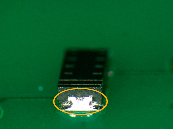
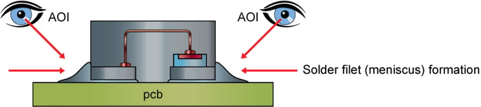
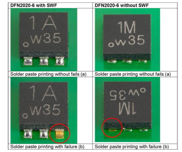
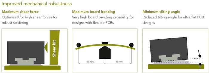
Creating a complete virtual model of a robot or system by simulating components and control programs can significantly impact the general efficiency of a project. Depending on the level of detail and accuracy of the simulation environment there are various areas which can be analyzed, all of which affect the development life cycle to a certain extent and of course cost.
Benefits of simulation
- Reduce costs involved in robot production;
- Diagnose source code that controls a particular resource or a mix of resources;
- Simulate various alternatives without involving physical costs;
- Robot or components can be tested before implementation;
- Simulation can be done in stages, beneficial for complex projects;
- Demonstration of a system to determine if is viable or not;
- Compatibility with a wide range of programming languages;
- Shorter delivery times.
Disadvantages of simulation
- An application can simulate just what it is programmed to simulate – it will not simulate internal or external factors which are overlooked in the development phase;
- A robot can encounter many more scenarios in the real world than there can be simulated.
New versions of simulation software platforms offer increasingly more features that make simulation easier and also very close to real life. Most simulation tools are compatible with programming languages like C/C++, Perl, Python, Java, LabVIEW, URBI or MATLAB, however they offer broadly varied feature sets depending on their purpose or focus areas. Take a look at the selection below to find the one which best suits your requirements.
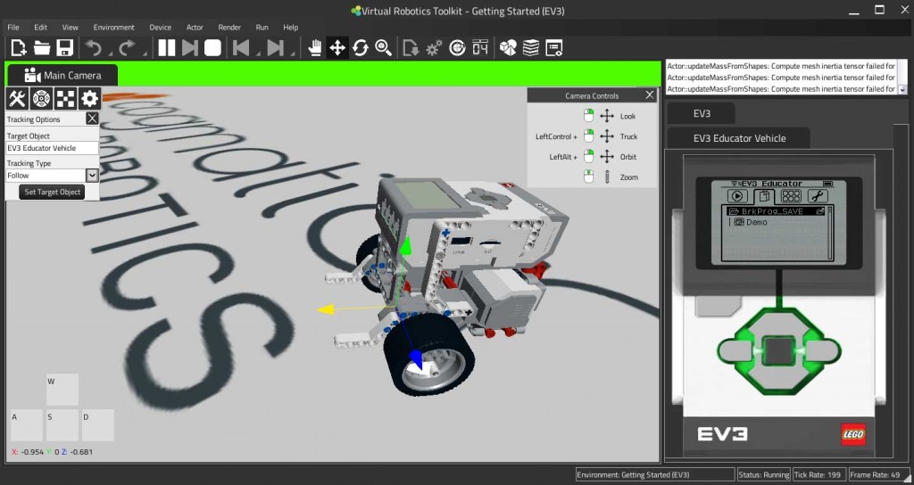
Virtual Robotics Toolkit
![Virtual Robotics Toolkit]()
Virtual Robotics Toolkit from Cogmation Robotics is a simulator for LEGO Mindstorms or VEX robots, depending on the chosen version. The product is focused on STEM education and is also useful for teams who want to prepare for robotics competitions. It supports importing 3D models from LEGO Digital Designer or other similar tools while programming the virtual intelligent brick takes place as in real life. The software runs on Windows and is available either as a single seat, team or class license. In the Mindstorms edition review there is more about this product.
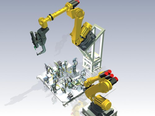
Visual Components
![Visual Components Production Line Simulation]()
Visual Components comes from Finland and is an advanced design and simulation suite for production lines. Entire manufacturing processes can be simulated and analyzed, including robotics equipment, material flow, human operator actions and more. The flagship product of the series
3DAutomate even supports entire factory simulations. Other features include offline programming, open APIs, and extensive component library with over 1800 3D models of industrial robots, machinery, facilities, tools and other hardware found in a factory, in my review you can read more about this.
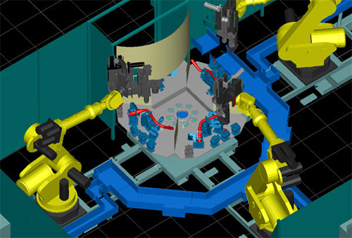
RoboDK
![Industrial Robot Machining Simulation]()
RoboDK is an offline programming tool for industrial robots which allows for scripting using Python or creating programs visually thanks to its integrated 3D simulation environment. All programs are automatically converted into robot specific languages before uploading them to physical robots. The software library offers 3D models for over 200 industrial robots and tools from ABB, KUKA, Yaskawa to mention just a few of them.
RoboDK provides numerous development features – it can generate alerts when robot singularities or possible collisions are detected, it represents graphically the robot work space, and also allows the user to have an overview of the whole technological and program accordingly. Head to my RoboDK review to find out more.
Robot Virtual Worlds
Robot Virtual Worlds is an advanced simulation software built around the powerful ROBOTC IDE. Users can program virtual LEGO Mindstorms NXT, EV3, VEX or TETRIX robots, either by using ROBOTC or visually via the Graphical Natural Language library extension, and observe their behavior in the 3D simulation environment which accurately renders these robots and their interactions. RVW was primarily designed as an educational tool however it is well suited for all levels of expertise – beginners can learn how to program these robots, teachers and students can use it for home or lab work, while advanced users can refine code or detect errors in their programming.
Several software extensions complement the feature set even further. For instance the Virtual Brick Emulator offers users a similar experience to that of programming an actual LEGO Mindstorms brick with NXT-G or LabVIEW. There are also extensions for creating custom levels, importing 3D models or measuring distances and trajectory angles around virtual environments.
RVW runs on Windows and is available in platform specific releasese. Free trial versions are available for download and licensing starts at US $49. There are also several apps available for iPad in which users can program VEX robots or play games with simulated robot behavior based on user programming.
Microsoft Robotics Developer Studio
![mrds]()
Microsoft offers robot developers a complete tool that can be used to program and create 3D simulations of your robot and environment.
MRDS 4 supports major robotic platforms like LEGO Mindstorms, VEX or various hardware such as the HiTechnic sensors and many more. The software offers various methods and technologies for rapid prototyping and includes a great amount of functional libraries.
Unfortunately as of September 22nd, 2014 Microsoft has suspended its Robotics research division, leaving MRDS 4 as the last released version of the software. Naturally this means that support is fairly limited and found on online communities.
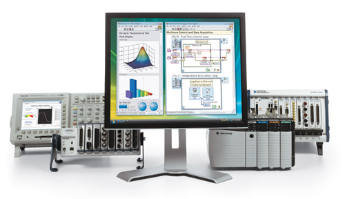
LabVIEW
![LabVIEW]()
Developed by National Instruments
LabVIEW is a cross-platform design and development environment built around the namesake graphical programming language. The first version of the product was released in 1986 and currently extensively used in education, engineering and research environments.
This is a complex ecosystem well suited for control, simulation, automation, data acquisition, analysis, measurement and many other purposes. Large model libraries are available for simulating a vast array of hardware components and interfacing with most standard interfaces in use today is very well supported. LabVIEW is a proprietary product however there are countless open source extensions for easy integration with other systems and software.
V-REP
![V-REP]() V-REP
V-REP is a 3D simulator compatible with Windows, Mac and Linux and is available either with a free educational educational license or with a paid license for commercial purposes.
The software allows modeling of an entire system or only certain components like sensors, mechanisms, gearing and so on. The control program of a component can be attached to the object or the scene with objects to model in a way similar to reality. The platform can be used to control the hardware part, develop algorithms, create factory automation simulations, or for educational demonstrations.
Webots
![Webots]() Webots
Webots has been created by Swiss company Cyberbotics. It has a friendly interface and supports languages like C/C++, Java, Python, URBI, MATLAB and can interface with third party software through TCP/IP. It is one of the most common simulation platforms with a long list of components which can be used in simulation and the possibility of adding other components. The software is cross-platform and trial versions are available.
RobotStudio
![ABB RobotStudio]() RobotStudio
RobotStudio is a powerful development suite created by ABB and is focused on industrial robot simulation and offline programming. The product also offers a generous list of components which can be used to simulate a robot or its sensors, actuators, grippers and more. A free version with limited functionality is available for download.
Gazebo
Gazebo can simulate complex systems and a variety of sensor components. It is used especially in developing robots used in interaction, to lift or grab objects, to push, or any other activity which requires recognition and localization in space. It is an open source software platform for which anyone can develop a plug-in with model components, also compatible with ROS and Player. Gazebo is open source and runs on Linux, ported versions for Mac and Windows are also available.
Actin Simulation
Actin Simulation has been created by Energid Technologies, an American company focused on developing integrated control solutions for robotics systems used in a broad range of industries such as aerospace, medical, transportation, manufacturing and many more. The software is part of the Actin control and simulation suite which can greatly reduce the time and cost associated with the development life cycle of projects employing robotics equipment, as well as optimize existing processes and workflows regardless of the level of customization. A wide range of mainstream industrial robots are supported by default however custom robots and configurations can be modeled, simulated and analyzed to virtually any extent.
Workspace
![Workspace]() Workspace
Workspace is a 3D simulation environment supporting a long list of languages used by industrial robot manufacturers such as ABB G-Code, ABB Rapid, Adept V-Plus, Fanuc Karel 5, Fanuc TP, Mitsubishi PA10, Mitsubishi Melfa Basic, Motoman Inform II, Kawasaki AS, Kuka KRL, Nachi Slim, Panasonic Pres and Siemens G-Code. Components and fixtures are included and can be used in building the simulation environment and robot.
Another important feature is compatibility with CAD files that can be created in other programs such as AutoCAD and imported for use in simulations. It is available either as an educational or commercial version and runs under Windows. Demo versions need to be requested from the developer.
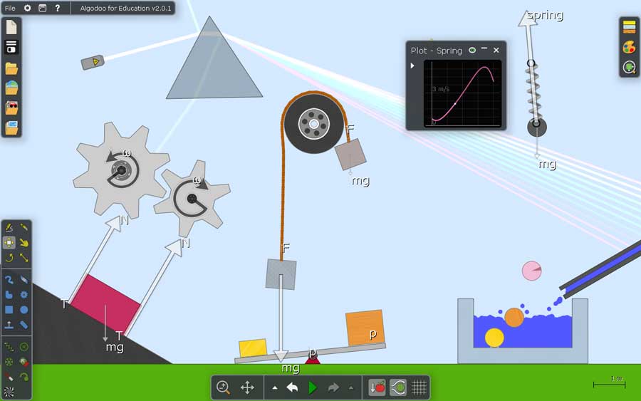
Algodoo
![Algodoo]() Algodoo
Algodoo is a free 2D simulation platform for educational purposes created by Swedish company Algoryx Simulation. It is used similarly as a drawing tool and is available for Windows, Mac and as a mobile app for the iPad.
EZPhysics
![EZPhysics]() EZPhysics
EZPhysics is a free open source software for Windows which allows for 3D simulation and animation in a similar way to video games. A set of examples, complete with accessible source code is included. Remote network interactions with the software are possible, and integration with MATLAB is also possible.
RoboLogix
![RoboLogix]()
With a friendly interface,
RoboLogix is an advanced 3D simulation environment for industrial robots,it is designed primarily as an educational tool however it can also serve well the purposes of engineers and robot designers. Some of the features include testing and editing programs used to control robots, and the possibility to optimize the cycle times by comparing the control programs. Free evaluation versions are available.
WorkcellSimulator
![WorkcellSimulator]() WorkcellSimulator
WorkcellSimulator comes from Italy and can be used to simulate and program industrial robots. It is mainly used for applications which involve handling, sorting or machinery for laser cutting and similar applications.
Roboguide
![Roboguide]() Roboguide
Roboguide is a software suite developed by FANUC Robotics consisting of four components, each of them having a role in simulation. HandlingPRO allows 3D simulation, PaintPRO is used to create links between robot components and programs, PalletPRO and PalletTool used for development and integration of robotic palletizing and depalletizing systems, and WeldPRO allows environment simulation where the robot operates. More information can be requested from the manufacturer.
It seems that the software products presented below have not been maintained in a very long time or have been integrated into other products. They is worth mentioning because most of them are still fully functional, some being based on pretty solid physics engines and can still serve well as educational tools.
OpenHRP3 is a complex environment based on a very realistic physics engine for dynamics simulation. Unfortunately there have not been any updates or maintenance for several years so it will probably remain in this development stage.
SimRobot is developed by Bremen University and used for research of autonomous robots. Current version is compatible with Windows, Linux and Mac OS X.
Simbad is a Java-compatible simulation tool that can be used for educational or scientific purposes. Simbad is mainly used for simulating 3D visualization and sensing, range or contact sensors.
Player is mainly used to simulate sensor applications. Compatible with most operating systems and programming languages, the platform can simulate a variety of sensors and their response to various stimuli. It also offers the possibility to create 3D simulations.
robotSim:Edu was part of the STEM suite created by Cogmation Robotics. It is no longer maintained as a standalone product being succeeded by Virtual Robotics Toolkit, mentioned earlier in the article.
RoboWorks 3.0 is an excellent 3D modeler for use in educational purposes and in industrial simulation. Graphics in 3D can be added in an easy way and it is compatible with C, C++, C/C++ interpreter Ch, VB, VB.NET, LabVIEW etc. It is available as a free demo.