Quantcast
Channel: LEKULE
Viewing all 1099 articles
Browse latest View live

Fuses

$
0
0
 Normally, the ampacity rating of a conductor is a circuit design limit never to be intentionally exceeded, but there is an application where ampacity exceedence is expected: in the case of fuses.

A fuse is nothing more than a short length of wire designed to melt and separate in the event of excessive current. Fuses are always connected in series with the component(s) to be protected from overcurrent, so that when the fuse blows (opens) it will open the entire circuit and stop current through the component(s). A fuse connected in one branch of a parallel circuit, of course, would not affect current through any of the other branches.

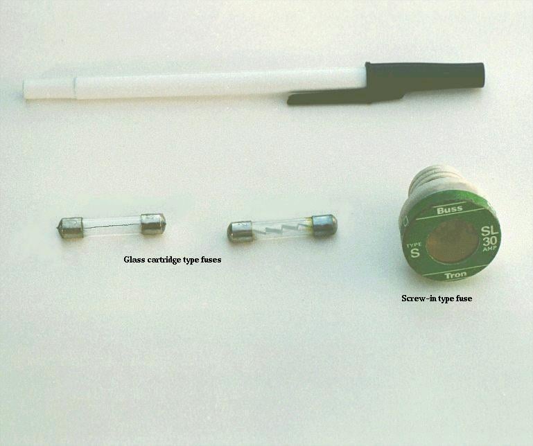
Normally, the thin piece of fuse wire is contained within a safety sheath to minimize hazards of arc blast if the wire burns open with violent force, as can happen in the case of severe overcurrents. In the case of small automotive fuses, the sheath is transparent so that the fusible element can be visually inspected. Residential wiring used to commonly employ screw-in fuses with glass bodies and a thin, narrow metal foil strip in the middle. A photograph showing both types of fuses is shown here:


Cartridge type fuses are popular in automotive applications, and in industrial applications when constructed with sheath materials other than glass. Because fuses are designed to “fail” open when their current rating is exceeded, they are typically designed to be replaced easily in a circuit. This means they will be inserted into some type of holder rather than being directly soldered or bolted to the circuit conductors. The following is a photograph showing a couple of glass cartridge fuses in a multi-fuse holder:


The fuses are held by spring metal clips, the clips themselves being permanently connected to the circuit conductors. The base material of the fuse holder (or fuse block as they are sometimes called) is chosen to be a good insulator.

Another type of fuse holder for cartridge-type fuses is commonly used for installation in equipment control panels, where it is desirable to conceal all electrical contact points from human contact. Unlike the fuse block just shown, where all the metal clips are openly exposed, this type of fuse holder completely encloses the fuse in an insulating housing:


The most common device in use for overcurrent protection in high-current circuits today is the circuit breaker. Circuit breakers are specially designed switches that automatically open to stop current in the event of an overcurrent condition. Small circuit breakers, such as those used in residential, commercial and light industrial service are thermally operated. They contain a bimetallic strip (a thin strip of two metals bonded back-to-back) carrying circuit current, which bends when heated. When enough force is generated by the bimetallic strip (due to overcurrent heating of the strip), the trip mechanism is actuated and the breaker will open. Larger circuit breakers are automatically actuated by the strength of the magnetic field produced by current-carrying conductors within the breaker, or can be triggered to trip by external devices monitoring the circuit current (those devices being called protective relays).

Because circuit breakers don’t fail when subjected to overcurrent conditions—rather, they merely open and can be re-closed by moving a lever—they are more likely to be found connected to a circuit in a more permanent manner than fuses. A photograph of a small circuit breaker is shown here:


From outside appearances, it looks like nothing more than a switch. Indeed, it could be used as such. However, its true function is to operate as an overcurrent protection device.


It should be noted that some automobiles use inexpensive devices known as fusible links for overcurrent protection in the battery charging circuit, due to the expense of a properly-rated fuse and holder. A fusible link is a primitive fuse, being nothing more than a short piece of rubber-insulated wire designed to melt open in the event of overcurrent, with no hard sheathing of any kind. Such crude and potentially dangerous devices are never used in industry or even residential power use, mainly due to the greater voltage and current levels encountered. As far as this author is concerned, their application even in automotive circuits is questionable.

The electrical schematic drawing symbol for a fuse is an S-shaped curve:


Fuses are primarily rated, as one might expect, in the unit for current: amps. Although their operation depends on the self-generation of heat under conditions of excessive current by means of the fuse’s own electrical resistance, they are engineered to contribute a negligible amount of extra resistance to the circuits they protect. This is largely accomplished by making the fuse wire as short as is practically possible. Just as a normal wire’s ampacity is not related to its length (10-gauge solid copper wire will handle 40 amps of current in free air, regardless of how long or short of a piece it is), a fuse wire of certain material and gauge will blow at a certain current no matter how long it is. Since length is not a factor in current rating, the shorter it can be made, the less resistance it will have end-to-end.

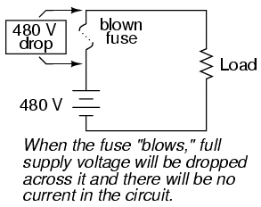
However, the fuse designer also has to consider what happens after a fuse blows: the melted ends of the once-continuous wire will be separated by an air gap, with full supply voltage between the ends. If the fuse isn’t made long enough on a high-voltage circuit, a spark may be able to jump from one of the melted wire ends to the other, completing the circuit again:


Consequently, fuses are rated in terms of their voltage capacity as well as the current level at which they will blow.

Some large industrial fuses have replaceable wire elements, to reduce the expense. The body of the fuse is an opaque, reusable cartridge, shielding the fuse wire from exposure and shielding surrounding objects from the fuse wire.


There’s more to the current rating of a fuse than a single number. If a current of 35 amps is sent through a 30 amp fuse, it may blow suddenly or delay before blowing, depending on other aspects of its design. Some fuses are intended to blow very fast, while others are designed for more modest “opening” times, or even for a delayed action depending on the application. The latter fuses are sometimes called slow-blow fuses due to their intentional time-delay characteristics.

A classic example of a slow-blow fuse application is in electric motor protection, where inrush currents of up to ten times normal operating current are commonly experienced every time the motor is started from a dead stop. If fast-blowing fuses were to be used in an application like this, the motor could never get started because the normal inrush current levels would blow the fuse(s) immediately! The design of a slow-blow fuse is such that the fuse element has more mass (but no more ampacity) than an equivalent fast-blow fuse, meaning that it will heat up slower (but to the same ultimate temperature) for any given amount of current.


On the other end of the fuse action spectrum, there are so-called semiconductor fuses designed to open very quickly in the event of an overcurrent condition. Semiconductor devices such as transistors tend to be especially intolerant of overcurrent conditions, and as such require fast-acting protection against overcurrents in high-power applications.


Fuses are always supposed to be placed on the “hot” side of the load in systems that are grounded. The intent of this is for the load to be completely de-energized in all respects after the fuse opens. To see the difference between fusing the “hot” side versus the “neutral” side of a load, compare these two circuits:


In either case, the fuse successfully interrupted current to the load, but the lower circuit fails to interrupt potentially dangerous voltage from either side of the load to ground, where a person might be standing. The first circuit design is much safer.

As it was said before, fuses are not the only type of overcurrent protection device in use. Switch-like devices called circuit breakers are often (and more commonly) used to open circuits with excessive current, their popularity due to the fact that they don’t destroy themselves in the process of breaking the circuit as fuses do. In any case, though, placement of the overcurrent protection device in a circuit will follow the same general guidelines listed above: namely, to “fuse” the side of the power supply not connected to ground.

Although overcurrent protection placement in a circuit may determine the relative shock hazard of that circuit under various conditions, it must be understood that such devices were never intended to guard against electric shock. Neither fuses nor circuit breakers were designed to open in the event of a person getting shocked; rather, they are intended to open only under conditions of potential conductor overheating. Overcurrent devices primarily protect the conductors of a circuit from overtemperature damage (and the fire hazards associated with overly hot conductors), and secondarily protect specific pieces of equipment such as loads and generators (some fast-acting fuses are designed to protect electronic devices particularly susceptible to current surges). Since the current levels necessary for electric shock or electrocution are much lower than the normal current levels of common power loads, a condition of overcurrent is not indicative of shock occurring. There are other devices designed to detect certain shock conditions (ground-fault detectors being the most popular), but these devices strictly serve that one purpose and are uninvolved with protection of the conductors against overheating.

  • REVIEW:
  • A fuse is a small, thin conductor designed to melt and separate into two pieces for the purpose of breaking a circuit in the event of excessive current.
  • A circuit breaker is a specially designed switch that automatically opens to interrupt circuit current in the event of an overcurrent condition. They can be “tripped” (opened) thermally, by magnetic fields, or by external devices called “protective relays,” depending on the design of breaker, its size, and the application.
  • Fuses are primarily rated in terms of maximum current, but are also rated in terms of how much voltage drop they will safely withstand after interrupting a circuit.
  • Fuses can be designed to blow fast, slow, or anywhere in between for the same maximum level of current.
  • The best place to install a fuse in a grounded power system is on the ungrounded conductor path to the load. That way, when the fuse blows there will only be the grounded (safe) conductor still connected to the load, making it safer for people to be around.

Understanding the Details of Fuse Operation and Implementation

$
0
0

The Basics

A fuse is a simple and highly effective way to protect a device from dangerous levels of current:
  1. Current flowing through a conductor’s nonzero resistance leads to power dissipation.
  2. Power is dissipated in the form of heat.
  3. Heat raises the temperature of the conductor.
  4. If the combination of current amplitude and duration is sufficient to raise the temperature above the fuse’s melting point, the fuse becomes an open circuit and current flow ceases.
Though the fundamental operation of a fuse is not complicated, there are subtle points to keep in mind. The rest of this article will help you to understand some important details related to the behavior and use of fuses.

Heat, Not Current

A fuse is not tripped directly by current; rather, the current creates heat, and heat trips the fuse. This is actually a rather important distinction because it means that fuse operation is influenced by ambient temperature and by the temporal characteristics of the current.

The specified current rating of a fuse is relevant only to a specific ambient temperature (usually, or maybe always, 25°C), and consequently you need to adjust your fuse selection if you’re designing a device that will operate outdoors in, say, Antarctica or Death Valley. The following plot shows how ambient temperature affects the actual current rating—relative to the nominal 25°C current rating—of three types of fuses.


Plot taken from this document published by Littelfuse.

Regarding the temporal characteristics of the current passing through the fuse, we all know that the effect of heat accumulates over time (momentarily touching a hot skillet is nothing compared to picking it up and realizing that it’s hot when you’re halfway between the stove and the dining table). Consequently, the current rating of a fuse is a simplification of its real behavior. We can’t expect a fuse to respond to high-amplitude transients because the short duration of the higher power dissipation doesn’t increase the temperature enough to cause tripping.

The following plot shows the time–current characteristics for a group of surface-mount fuses made by Panasonic. The rated current is on top, and the curve represents the amount of time required to trip the fuse in relation to the amount of current flowing through the fuse.


Plot taken from this datasheet.

As you can see, transient amplitudes must be much higher than the rated current. For example, you need 3 amps to trip a 0.5-amp fuse when the duration of the overcurrent condition is only 1 ms.

Connect Them In Series!

I’m not going to dwell on this point because it’s so straightforward, but it’s worth mentioning just in case you’re up late designing a schematic and in your exhausted state you don’t notice that you placed the fuse in such a way that it is, for example, in series with only one of two voltage regulators. A fuse cannot protect anything that is connected in parallel with it.

Rated Current vs. Operating Current

It would be perfectly reasonable to assume that a fuse rated for 6 amps could be used in a circuit that might need 5 amps of steady-state current. It turns out, though, that this is not good design practice. The current rating of a fuse is not a high-precision specification, and furthermore (as discussed above) the actual tripping current is influenced by ambient temperature. Consequently, to avoid “nuisance tripping,” you should have a fairly generous gap between your expected steady-state current and your fuse’s rated current. This document from Littelfuse suggests a “rerating” of 25% (for operation at room temperature); thus, a fuse with a rating of 10 amps would be used only if the circuit’s steady-state current will stay below 7.5 amps.

You Have to Be Patient

Let’s say your circuit includes a delicate component that will certainly be damaged if it is subjected to currents higher than 1 amp. The circuit should never draw more than 500 mA under normal conditions, so you include a fuse with a rating of 900 mA. This is high enough to prevent nuisance tripping and low enough to ensure that the delicate component never sees 1 amp. Right?
Well, no. Consider the following spec for the Panasonic fuses mentioned earlier in the article:


Image taken from this datasheet.

We’ve already discussed the fact that heat takes time to accumulate, and in this case it takes a long time: you’ll have to wait at least four hours for the fuse to trip when the current is equal to the rating, and even at twice the rated current the delay is at least five seconds. The bottom line is that the delicate component might be toast long before the fuse trips. You’ll have to rethink your fuse selection or—and this is probably a more practical solution in a situation such as the one described above—implement a different method of dealing with overcurrent conditions.

Don’t Forget About Voltage

Fuses are designed to have very low resistance so that they don’t unduly interfere with the circuits that they are protecting. This low resistance means that the voltage drop across the fuse will be very small. Why, then, do fuses have a voltage rating?

It’s true that fuses see small voltage during normal operation, but the voltage rating is not relevant to normal operation. Rather, the voltage rating tells you what the fuse can endure after it has tripped. A blown fuse is an open circuit, and if the voltage across this open circuit is enough to cause arcing, the fuse can’t be relied upon.

It’s a good idea to keep an eye on voltage ratings if you’re using tiny surface-mount fuses, such as the one shown below (note how thin the actual fusing element is). The rating for an 0603 fuse, for example, could be 32 V or even 24 V.


Diagram taken from this datasheet.

Conclusion


We’ve covered some interesting details about how fuses work and how to effectively incorporate them into our designs. In a future article we’ll explore the different types of fuses.

AIRBUS A380-800-R: New technologies

$
0
0

Revenue generation

The A380’s service introduction ushered in a new era of airline transportation for operators. Whether it’s being used to reduce the number of flights and create cost savings while maintaining capacity, or to offer more capacity with fewer takeoff slots, the A380 brings operators a wide range of commercial advantages. Furthermore, with two full-length decks, more space for every passenger, and a flying experience no other aircraft in the sky can match, the A380 has become a must-have ticket on every route it flies – resulting in a significant first-mover advantage for operators.

New technologies

A380 Airbus cockpit
A380 Cockpit
The A380’s cockpit – which is based on Airbus’ industry-leading flight deck design for its fly-by-wire jetliner families – features the latest advances in cockpit technology, including larger interactive displays, an advanced flight management system and improved navigation modes.

The A380's main instrument panel incorporates eight identical and interchangeable Liquid Crystal Display Units, providing a primary flight display, navigation display, two multi-function displays, an engine warning display and a systems display. The increased display size provides increased perspective for pilots and allows for enhanced presentation modes as a vertical situation awareness function that presents a “vertical cut” of the aircraft trajectory incorporating flight path, terrain and weather information.

A key A380 innovation is the use of an electronic library to largely replace the traditional paper documentation used by pilots. This library allows flight and maintenance crews to easily locate relevant operational information in the various flight manuals, lists and logbooks, while enabling an optimisation of performance and weight-and-balance computations.


Technology A380

Runway management

455
Airbus introduced its innovative Brake to Vacate technology on the A380, allowing flight crews to more effectively manage approach and landing by pre-selecting the optimum runway exit. This can reduce runway occupancy time by up to 30 per cent – significantly increasing the number of aircraft that can be handled by the world’s airports.


Advanced materials

Industry agreement signed at ICAO Assembly
By incorporating the latest advances in structures and materials, the A380 offers the lowest cost per seat of any widebody aircraft, over 15 per cent lower than its nearest competitor. This includes the use of advanced aluminium alloys for the wing and fuselage,

along with the extensive application of composite materials in the centre wing box’s primary structure, wing ribs, and rear fuselage section.

The A380 also uses Glare™ material in the pressurised fuselage’s upper and lateral shells. Glare™ is a laminate incorporating alternate layers of aluminium alloy and glass fibre reinforced adhesive, with its properties optimised by adjusting the number of plies and orientation of the glass tapes. This offers a significant reduction in weight and provides advanced fatigue and damage resistance characteristics.


Efficiency and reliability

A380plus Featuring New Large Winglets Day0 PAS2017
At the 2017 Paris Air Show, an A380 flight test aircraft was displayed with the new large winglets conceived by Airbus as part of aerodynamic refinements for the A380plus version

Two new-generation engine options (the Engine Alliance GP7200 and Rolls-Royce Trent 900), combined with an advanced wing and landing gear design, make the A380 significantly quieter than today's largest airliner – enabling this very large aircraft to meet strict local regulations at airports around the world.

With a new wing design and composite materials accounting for 25 per cent of its structural weight, the A380 is the most efficient aircraft all around. By producing only about 75 grams of CO2 per passenger kilometre, the A380 is helping the aviation industry's commitment to minimise greenhouse gas emissions.

A380 reliability and maintainability is further increased with modern technology, including an enhanced onboard central maintenance system and variable frequency generators – which simplify the large aircraft’s electrical generation network. Hydraulic power is provided by two fully independent systems with an operating pressure of 5,000 psi., instead of the conventional 3,000 psi. This capacity for higher pressure results in smaller and lighter hydraulic system equipment, as well as less hydraulic fluid on board, proving how Airbus innovations continue to deliver efficiency in every area of aircraft design and manufacture.


The interactive map above highlights the optimised range of this modern Airbus jetliner. To determine the aircraft’s range from a specific location, simply drag the cursor to any city or region. The area covered in blue will represent all possible destinations within its typical range.

Note: The range areas above illustrate the aircraft's nominal range.

Transformer Oil Purification Systems

$
0
0
Duke 250 banner
Present and future transformer ratings require high quality and high purity insulating oils at the point of use. The increasing voltage and rating of the modern transformer and electrical apparatus results in greater electrical stress in insulating material and fluids. To handle these greater stresses, oils with better dielectric qualities are required. Also lower residual water content in insulating fluids and material must be maintained. The proper treatment and upgrading of the insulating fluid will result in the improvement of the properties of the entire insulating media of power transformers. The principal functions of the insulating fluid are to serve as a dielectric material and as an effective coolant. To perform these functions, the insulating fluid must have the necessary qualities at the time of initial impregnation and filling at the factory and later maintain the same quality in the field operation. ENERVAC’s High Vacuum Process upgrades the new or used electrical insulating fluids including transformer oils, polybutenes and silicone fluids. These systems and equipment were developed as a result of 50 years of experience in vacuum treatment of electric insulating fluids.

NEW– ENERDry-Transformer Dry-Out SystemNEW

Enerdry
  • Extends service life of transformer by extending the service life of the insulating system (paper & oil).
  • Transformer remains in service during processing (no lost revenue due to down time).
  • Reduced processing costs in relation to other processes.
  • Maintains low moisture levels in transformers in service.

Transformer Oil Purifier / Degasification (E865A) High Performance

  • Upgrading of new and used electrical insulating liquids, transformer oils & silicones.
  • High Vacuum process removes free and soluble water.
  • Removes free and dissolved gases and particulate matter.
  • Mobile and stationary units available in sizes from 50 to 6,000 GPH.

Transformer Oil Purifier / Degasification (EHV)

  • Upgrading of new and used electrical insulating liquids, transformer oils & silicones.
  • High Vacuum process removes free and soluble water.
  • Removes free and dissolved gases and particulate matter.
  • Mobile and stationary units available in sizes from 200 to 23,000 l/h.

Portable Transformer Oil Purifier/Degasifier (E865C)

Portable transformer oil purifier filter Degasifier (E865C)OK
  • Mounted on a hand cart with 10″ (25 cm) pneumatic tires.
  • Connection provided for vacuum controller.
  • Pump blank off pressure 20 micron.
  • Operates unattended.

Mobile Circuit Breaker Oil Purifier (E858M)

Mobile circuit breaker oil purifier filter (E858M)
  • Extend the life of oils used in transformers, circuit breakers, voltage regulators and switch gear.
  • Completely mobile and certified for highway travel.
  • Cart will retrieve the fluid, flush and fill oil filled circuit breakers.
  • Removes carbon, water and particulates from oil.

On-Line Tap Changer Oil Purifier (TFS-2)

On-Line tap changer oil purifier filter (TFS-2)
  • Reduces carbon, water and metallic particles in tap changers.
  • Operation and maintenance costs are reduced.
  • Dielectric strength of the oil remains high.
  • Contact wear and coking is reduced.

Insulating Oils Purification Fuller’s Earth Filter (E575A)

  • Removes acids and soluble surface acting contaminants by adsorption.
  • Increases the IFT of the oil and reduces PF (Power Factor) to desired levels.
  • Positive protection assures migration-free, sparkling clean effluent.
  • Various sizes and configurations are available, mobile or stationary.

Transformer Oil Regeneration Plant (E575R)

ENERVAC’s Transformer Oil Regeneration Plant provides all the benefits of Fuller’s Earth treatment without the associated problems of contaminated clay disposal or the high cost of replacing saturated earth. At the end of the useful lifetime of the regeneration media, normally 300 times longer than Fuller’s Earth, it is simply disposed of in a normal landfill site. Ideally suited to large throughputs, the plant is available in either a mobile or stationary version.

Electrical Transformer Oil Purifier / Poly Chlorinated Biphenyl (PCB) Decontamination

PCB Destruction Unit
  • Cost effective destruction of P.C.B.’s, Patented technology.
  • Restores oil for reuse.
  • Reclassifies transformers.
  • Totally enclosed mobile system, EPA / MOE approved.

Cascade Refrigerated Cold Trap E861B

Cold Trap (2)
  • Unit is designed to trap condensable vapours (usually water) during transformer drying process
  • Capable of pressures in the low micron range and a plate temperature of -85°F
  • Provides fast dry-out of “wet” transformers

High Efficiencies, Small Package: An Integrated Boost (Step-Up) Module Regulator from Analog Devices

$
0
0
Linear Tech's new boost (step-up) module regulator comes in a small BGA package and offers high efficiencies.

Linear Technology, now part of Analog Devices, has announced their new boost (step-up) µModule regulator, the LTM4661.


Image from the datasheet (PDF).

This power module operates from input voltages ranging from 1.8 V to 5.5 V, and is able to continue operation with an input voltage as low as 0.7 V after startup. Seems impressive!

This IC can generate output voltages ranging from 2.5 V to 15 V with continuous output currents up to 2 amps (see the figure below). According to the datasheet, in the section entitled Output Current Capability (page 8), the actual "output current capability depends highly on the input/output voltage ratio."

Also, be sure to pay close attention to the current-derating curves, when viewing the maximum output current values, and make use of the equations on page 8 when designing your circuit.


As can be observed, the maximum continuous output current of 2 amps is only possible at a VOUT of less than or equal to 5 volts. Table from the datasheet (PDF).

Because of its integrated design nature, only a few bulk capacitors are required, at a minimum, for operation. For instance, when a VOUT of 1.2 volts is desired, no voltage-setting resistor is necessary (see the following figure). And when a VOUT other than 1.2 volts is required, only one resistor is needed.

The following figure, which includes a table for selecting the VFB resistor value, illustrates how easy and straightforward it can be to utilize this IC. For more information on setting the IC's output voltage, check out the section entitled Output Voltage Programming (page 8) in the datasheet.
 

Depending on design requirements, using the LTM4661 may only require external bulk capacitors. Image and table taken from the datasheet (PDF).

What is a "µModule Regulator"?

Now, if you're an active reader of these types of articles from LEKULE BLOG, then the phrase "µModule Regulator" may look familiar. In fact, we referenced this phrase, as in the "µModule buck regulator," in a previous article that discussed Linear Tech's LTM8063. The LTM8063, which is a step-down (buck) regulator, should not be confused with the LTM4661—which, again, is a step-up (boost) regulator.

The term µModule, which is a registered trademark, serves seemingly as Analog Devices' catch-all label to describe their DC-to-DC fully-integrated system-in-package (SiP) power management solutions. So, when I say: "system-in-package (SiP) power management solutions," what I mean is that these modules contain the DC-to-DC controllers, the power switches, the compensation components, and the inductors, all within a compact BGA package.

Offers an Efficiency of up to 92%... Under Optimal Parameters

While this IC is said to offer efficiencies of up to 92%, which is indeed accurate, we must be mindful that these high-efficiency values are only attainable under specific parameters, such as VIN, VOUT, and IOUT (see the figure below).
 

These graphs illustrate the fact that attaining high efficiencies is a function of the ICs parameters. Plots taken from the datasheet (PDF).

It's interesting to note that the Burst vs. Continuous Mode Efficiency plot omits the VOUT value. So, should it be assumed that these high-efficiency values are valid irrespective of VOUT? If you have insights into this assumption, please share them in the comments section.

Based on common input and output values, Linear Tech has provided the following table for quickly identifying efficiency capabilities as a function of VIN and VOUT. For more information on current capacity, head over to the section entitled Output Current Capability on page 8 of the datasheet.
 

This table, from the datasheet, can be treated as a quick reference guide for determining efficiency levels as a function of common VIN and VOUT values.

Need More Current? Try Paralleling Multiple ICs

If your design requires more current than what's available from a single LTM4661 module, then consider adding additional parallel ICs. The following figure is an example of how two LTM4661 power modules are used in parallel.

An example of using two LTM4661 ICs in parallel. Taken from the Applications Information section on page 17 of the datasheet (PDF).

And, when it comes to selecting the voltage-setting resistor of paralleled ICs, simply use the provided equation (see figure below) on page 8 of the datasheet.
 

Linear Tech provides this simple equation for determining the voltage-setting resistor based on the number of paralleled ICs. Equation taken from the datasheet (PDF).

Evaluation Board

If you're interested in testing/playing with this new step-up/boost power module, there's a dev board available for the LTM4661, the DC2569A. Linear Tech/Analog Devices provides the demo board's design files and schematics and a demo board manual.

The DC2569A is a demonstration circuit (i.e., demo board) for the LTM4661 voltage boost IC. Image courtesy of Analog.com.


Have you had a chance to use this new voltage boost µModule regulator from Linear Tech/Analog Devices, or its demo board? If so, leave a comment and tell us about your experiences.

Great Scott! Stanford’s Self-Driving Delorean

$
0
0
If you're going to live in the future, you may as well have a sweet ride.

Today marks the day that Marty McFly will arrive from 1985 to save his future children. Ok, sure, we don't have true hoverboards or wear plastic strainers on our heads, but Stanford has stepped in to make our present a whole lot cooler: it's unveiled a self-driving DeLorean. Named after the Back to the Future protagonist, the MARTY (Multiple Actuator Research Test bed for Yaw control) doesn't just politely maneuver its way through stop-and-go traffic-- it can pull impressive drifts and hair-raising doughnuts better than an RC racer. Watch the video below to see the DeLorean in action.


Upgraded Components

Any EE worth his or her salt knows about the sensors that go into Google's car--the rogue DeLorean doesn't have radar or LIDaR sensors. It's basically a punk hack of Renovo's drivetrain coupled with a really good GPS system and two separate motors on the rear wheels that control the amount of torque delivered to each one. The motors can operate at 200 kilowatts of power-- not quite 1.21 gigawatts, but it'll do. The car uses mechanical engineering and autonomous driving software to navigate the hurdles of street driving.

Working with a 40-year-old car posed some basic issues to the Stanford team. They had to add power steering and a custom steer-by-wire, build a roll cage, then get Bridgestone to donate tires that could withstand drifting (and the ravages inflicted by a pack of tech geniuses).

The team inspects the DeLorean. Courtesy Stanford.

Why Drifting?

Thus far, autonomous cars have been relatively vanilla: we haven't seen them pull any maneuvers that normal drivers couldn't do. But what's the point of having self-driving cars if they don't drive better than humans can? Chris Gerdes, the professor of mechanical engineering behind the project, wanted to test the physical limits of autonomous driving because, he says, "We want to design automated vehicles that can take any action necessary to avoid an accident."

What would have happened if, back in July when Google's self-driving car got into its first accident with injuries, the car would have predicted the accident and pulled some sweet maneuvers to avoid it? A truly progressive autonomous car would be able to gauge the risk of becoming less stable but more agile versus increased stability with increased rigidity. In other words, the Stanford DeLorean can pull some racecar-driving moves to protect its occupants.

A Less Boring Future

Just about every model we've seen of autonomous cars has resembled a passive jelly bean that looks like it's meant to shuttle passengers to get overpriced quinoa salad. The designs have been more Elysium than Mad Max, and that points to a future that's playing it safe. The Stanford DeLorean hearkens back to a time when designs took risks. Does anyone need gull-wing doors? Debatable. Are they show-stoppers? Absolutey.


Beyond having just harnessed racing car tactics into self-driving practicality, the hacked DeLorean offers a reminder that the future shouldn't play it safe: we've come too far to let our cars look and act as boring as early morning traffic.

Teardown: Uniden CB Radio

$
0
0
In this teardown, we disassemble a CB radio, from Uniden, to see what interesting things we can find.

This professional CB radio—the Bearcat 680, by Uniden—allows for chitchatting on 40 different channels. It integrates both volume and squelch control on the same rotary-switching device, and provides a large channel-display, all in a fairly small form factor.


Uniden's Bearcat 680 CB radio looks easy-to-use given its large display and minimal controls.

Let the Disassembly Begin

Fortunately, gaining access to this unit's internal components is rather easy and straightforward since only a handful of Phillips and hex screws are used for holding everything together. In the figure below, we can begin to see, with the top sheet metal piece removed, that this CB radio uses multiple PCBs.


Our first glance inside the unit reveals the speaker and four PCBs.

Upon close inspection of the device's innards, we can see that the sparkies (i.e., the electrical engineers) and the wingnuts (the mechanical engineers) worked together and communicated closely and effectively by ensuring that the sheet metal mounting holes aligned properly with the associated PCB holes.

Also, as can be observed in the image below, two of the ICs make use of the sheet metal frame for their heat sink. Again, this design effort required collaboration... nice job, Uniden!


At this angle, we can see how the design nicely fits together.

Removing and Inspecting the Guts

In the figure below, we can clearly see four PCBs:
  • The main PCB, which is comprised of all the ICs and the CB radio's intelligence;
  • the display PCB, which connects to the main PCB via a simple ribbon cable;
  • and, two simple rotary switch PCBs—one for each of the control switches.
Using dedicated PCBs for each of the control switches is a solid design approach as it allows for, obviously, much more freedom and independence of where each of the switches can be located. An alternative approach—although perhaps a more cumbersome approach—would've been to solder these switches directly to the main PCB.


The four PCBs removed from the radio's enclosure.

The list below calls out some of the major components identified in the figure above:
  • Power MOSFET: Part marking IRF520
  • Audio Amplifier: Part marking UTC TDA2003L
  • Relay: Part marking HFD27/005-H
  • Voltage Regulator: Part marking L7808CV
  • Microcontroller: Part marking M38D58G8HP
  • Potentiometer: Part marking TOCOS A503 6502 57C
    • Note: This switch is a dual-switch, meaning that it is comprised of two independent rotary switches.
  • Rotary Switch: Park marking CTR SR476 1564C (similar to this part)
  • Frequency Synthesizer: Part marking MCD2926
  • CB Transceiver Driver: Part marking C2314
When viewing the PCBs' opposite sides (see image below), we can see that the PCB layout person/team did an excellent job by locating all (or most) of the main PCB's components on the PCB's top-side; it appears that the single axial resistor on the back side is most likely from a rework task.


The opposite sides of the PCBs and switches.

The display screen contains no part markings, which, in my experience, appears to be the norm for similar devices. And while the pushbuttons/tactile switches also have no markings, they appear to be similar to this part.

Conclusion

Although I did not actually use this Bearcat 680 CB radio prior to tearing it down, it does indeed look to be a solid design, both electrically and mechanically. And, given the use of multiple sheet metal mounting points, as well as hefty heat sinks for the hot ICs, this unit should provide years of service in a home or a big rig.


Do you have any experience with this particular CB radio? If so, please share in the comments section.

Accelerating Embedded Vision Integration with Xilinx SoCs and the reVISION Stack

$
0
0
FPGA design strategy is changing, especially in the sphere of embedded vision systems. New design solutions utilize software-based systems with integrated hardware acceleration, allowing faster development but also requiring new design methods and tools. Xilinx and Avnet have partnered to provide a comprehensive system environment to help designers keep up with these emerging trends.


SoCs with programmable logic are an essential element of real-time embedded vision systems. Designers can capitalize on the power and efficiency of Xilinx's Zynq Ultrascale+ MPSoC devices to implement their designs using Avnet's Embedded Vision Kits and the Xilinx reVISION stack.
This ecosystem enables a straightforward approach to integrating deep learning AI-based vision features and facilitates rapid development by eliminating software development dependency upon the first prototype hardware cycle.

Introducing computer vision to embedded design can be a complex process. Invariably the hardware must be small, lightweight, low power, and low cost. Fast product development cycles make known good solutions for the underlying functionality essential. Every minute spent on the lowest levels of the firmware is another minute not designing functionality that differentiates the product.
Xilinx provides a fully integrated solution that engineers can modify and build upon. Software engineers can get started on complex machine-learning-based image processing designs without writing a single line of hardware HDL code by using the SDSoC Development Environment, a Zynq Ultrascale+ MPSoC development kit, and one of the many complete design examples available.

Zynq Utrascale+ MPSoC

The rapid development of embedded vision products requires the use of an existing hardware platform with sufficient interfaces and onboard functionality to meet product requirements. The platform must also provide an easy-to-use, robust firmware and application development environment.

For this, Xilinx collaborates with Avnet. Avnet's experience with years of vision-oriented development cycles has culminated in a complete system approach including the Avnet Embedded Vision Kit with multiple SoC-based SoM options, video-specific carrier cards, and features like PoE. Designers can utilize Xilinx's development ecosystem to exploit programmable SoC device families like the Zynq Ultrascale+ MPSoC, enabling focus upon fine-tuning and customizing intellectual property rather than porting code.

Xilinx and Avnet stack concept.
Xilinx and Avnet work together to compliment embedded vision products with robust firmware and application development environments.

Today’s embedded vision products require single device solutions that are powerful enough to meet real-time task deadlines and critical mission safety specifications while staying within challenging power efficiency budgets. Video and image processing typically requires sophisticated features like object detection and recognition, algorithmic decision-making, and motion path selection. The outputs of these processes must be deterministically bound to control decisions, status analysis, and human-machine interface notification. Without such determinism, safety and reliability are directly impacted. Devices like the Zynq Ultrascale+ MPSoC feature four ARM Cortex-A53 CPUs that enable symmetric multiprocessing implementation upon image processing and application-rich operating systems like Linux.

The Zynq Ultrascale+ MPSoC further integrates essential functionality critical to embedded vision products with two ARM Cortex R5 real-time processors operating independently of the quad-core and operating system environment. This enables the implementation of lockstep monitoring and safety features that can continue operation in the event of a serious software system failure. A separate fault-tolerant platform management unit enables safety and power management functions while a configuration and security unit provides easy configuration and security threat protection. Finally, a Mali-400 graphics processor provides built-in 2D and 3D rendering, allowing the platform to provide for high-quality video display output.

The Zynq Ultrascale+ MPSoC are not simply FPGAs anymore. Xilinx has recognized a software-centric approach better meets the expectations of the embedded vision marketplace. FPGA design strategy has changed from proprietary hardware solutions requiring considerable investment in hardware HDL implementations to achieve real-time performance. Systems are now software solutions that require hardware acceleration increasingly provided by tried and tested off-the-shelf IP. Hardware acceleration integrates into software applications by future proofing frameworks like OpenCL. The reVISION stack is Xilinx's way of putting this all together in a complete system environment.

The reVISION Stack

Embedded vision systems need guided machine learning and computer vision acceleration. Xilinx 'all-programmable' technology utilizes the software-defined embedded vision 'reVISION stack' to realize machine learning, sensor fusion, and computer vision. The reVISION stack encompasses a software-defined environment inside an industry standard framework to enable implementation of most of the popular neural networks used today, including AlexNet, GoogLeNet, SqueezeNet, SSD, and FCN. Optimized reference models for these neural networks are available.

The reVISION stack also includes all the functional capability and blocks required to build completely custom neural networks. Neural networks are typically layers of convolutional (filter) and non-linear (activation) processes that may interpolate (upsample) or decimate (downsample) information from the previous layer. The reVISION stack accommodates most interface layering methods with hardware-optimized implementations of Conv, ReLU, Pooling, Dilated conv, Deconv, FC, Detector & Classifier, and SoftMax.

reVISION stack logo

Designers can choose from an array of image processing IP that seamlessly integrates with neural network capability under frameworks like Caffe and OpenVx. The result is high responsiveness and configurability with access to the resources of a wide development community of people continually adding and updating OpenCV libraries. With Xilinx OpenCV (xfopenCV) the most critical acceleration functions oriented toward applications like drone control, autonomous driving, and machine learning are immediately available.

Software developers can incorporate hardware accelerators like filters, image processing, and motion tracking with a few lines of well-documented code. Input data can easily be streamed in and out of these instantiations as simple objects being referenced like function parameters. Direct streaming is a powerful way to optimize the use of memory in a system. By using streaming in this way, the compiler can directly link acceleration modules using internal bus structures with minimum memory overheads and avoid external memory access. This reduces power consumption and leads to significant improvements in processing latency.

Platform Resources

If you need a platform to get started with, Avnet’s Zedboard is an online resource containing related examples, information, and training using a number of ready-made Zync SoC module (SOM) based kits. Designers can also utilize the reVISION stack in combination with development platforms like the Zynq Ultrascale+ MPSoC ZCU102 Evaluation Kit using FMC and USB interfaced cameras, HDMI sources and virtual video devices to both train and implement applications. The neural network-based system is easily customized through software running on the ARM processor system without the need of a time-consuming compilation process. Many design examples incorporating both machine learning and vision are available to learn from, including motion detection, face tracking, thermal imaging, and robotics applications.

Embedded Vision in the World

Multi-camera vision applications are becoming increasingly common. This is especially the case in Advanced Driver Assistance Systems (ADAS) where a platform must be capable of meeting the processing power required for the fast frame rates, high-performance signal processing, sophisticated sensor fusion, and dedicated neural network hardware acceleration. However, the problem goes beyond this into relatively simple criteria that can be frequently overlooked. It does not matter how powerful a device is if it does not meet the approval standards required for automotive applications.
Xilinx’s automotive qualifiedXA Zynq Ultrascale+ MPSoC family meets AEC-Q100 test specifications. This enables device use in harsh automotive environments that require higher temperature grades, high visibility change management, and high-reliability manufacturing. Above the physical and environmental specifications, these devices incorporate a 'safety island' that enables real-time processing to be implemented in mission-critical safety applications like ADAS, allowing device certification that meets the ISO 26262 ASIL-C standard.

As the previous example showed, it is important to factor in all the requirements essential to an embedded vision system before choosing a platform. The programmable logic available on the Zynq Ultrascale+ MPSoC devices enables solutions in systems where a CPU-only based solutions would be impractical and even dangerous. An example of this is in industrial robotic motor control applications. These typically require high-speed PID loops that base error calculation on real-world feedback requiring high-speed sampling of analog signals.

The programmable logic fabric available on the Zynq Ultrascale+ MPSoC devices works well in this role, reducing the needs for rapid interrupt task-based software drivers that can reduce system stability and degrade performance. Even if the control algorithm is simple, the real-time determinism required to maintain low jitter and the sample rates lead to rapid task switching, causing significant processing power wasted in the task switching alone.

Safety-critical embedded vision products like those in industrial robotics control require a failsafe operation. The Zynq Ultrascale+ MPSoC integrated system monitor includes a multi-channel ADC along with on-chip sensors that monitor on-die operating conditions such as temperature and supply voltages. This enables fault conditions to be detected independently from the software domain, with status available through external communication ports such as an I2C interface and alarm outputs. The Zynq Ultrascale+ MPSoC has an additional high-speed monitor capable of up to 1MSPS sampling (PDF), enabling extremely rapid response to fault conditions. Upon fault detection, the robotic control system can park itself in a safe state of operation protecting both equipment and user.

Conclusion

Xilinx Zynq Ultrascale MPSoCs are devices made easy to use due to the comprehensive reVISION stack and flexible, vision-oriented hardware development kits. An MPSoC has a clear advantage over embedded CPUs due to configurable programmable logic hardware acceleration. The result is a fully integrated embedded vision development system that utilizes a software-centric approach.
Xilinx has added functionality to support reconfiguration, reliability, monitoring, and safety, eliminating the need to bolt on additional supervisory hardware.

Existing examples enable designers with limited knowledge of FPGA logic design to get started. The use of OpenVx, Caffe, OpenCL, and OpenCV standards, along with an operating system like Linux, opens up any system development to a large pool of third-party IP to accelerate development and future-proof applications.


Implementing advanced vision features are possible with the Zynq Ultrascale+ MPSoC and reVISION. Solutions with Xilinx and Avnet can help cut through all the pain and suffering of complex system design and bring clarity projects: whether it’s an autonomous car, a medical imaging device, or the next-generation coffee stirring, dishwashing robotic super drone. Resources to help you discover more about how you can realize embedded vision solutions and read about other innovative successes including robotics and autonomous driving are available here.

Sensirion’s “World’s Smallest Flow Sensor” for Taking Accurate Differential Pressure Measurements

$
0
0
Sensirion announces their new SDP3x series of "the world's smallest differential pressure sensors," which allow for more integration and application possibilities.

Sensirion recently announced their new SDP3x series of differential pressure sensors.


A rather unique and specialized-looking pressure sensor. From the SDP3x datasheet (PDF).

As of the writing of this article, there are four IC versions within this series: two digital (I2C) sensors, and two analog output sensors. See the image below. And instead of cramming both the digital and analog sensor information into a single datasheet, Sensirion has made it a bit easier, at least in my opinion, by providing standalone documents of the digital version datasheet and the analog version datasheet. Keep in mind, however, that this article will focus only on the digital part.
 
Depending upon your application's needs, you can choose from either two digital (I2C) or two analog flavors. Information courtesy of Sensirion.com

This "world's smallest differential pressure sensor" is well-suited for applications such as smart inhalers (see image below), medical home care applications, and appliances.
 
The SDP3x allows for numerous new application possibilities, such as this smart inhaler. Image courtesy of Sensirion.com

CMOSens Technology

Like all other Sensirion products, the SDP3x series of pressure sensors use Sensirion's CMOSens Technology for fusing together the sensor element and the digital signal processing on a single CMOS chip. This technology approach, according to Sensirion, is what allows the SDP3x series sensors to provide both high reliability and long-term stability (see the image below). By the way, this pressure sensor also provides temperature readings. A nice add-on!
 

It's Sensirion's CMOSens Technology that allows for stable, reliable, and repeatable measurements (for both pressure and temperature). Table taken from the SDP3x datasheet (PDF).

Device Pinout

If, at first, you find yourself a bit intimidated when viewing the sixteen pins of this sensor (see image below), hopefully your apprehension will be diminished by the fact that five of these pins are no-connects and that six pins are for GND connections, leaving a mere five pins for routing.
The die pad is internally connected to ground and can be soldered to increase mechanical stability. However, and this is real important: be mindful that the hole in the middle of the die pad (center pad) must stay open during and after the soldering process. For more information on this topic, check out Section 3.6 (entitled Die Pad (Center Pad)) of the datasheet.
 

Only five of the sixteen pins, not counting GND, need to be routed. From the SDP3x datasheet (PDF).

I2C Interface, and Multiple I2C Addresses using a Single ADDR Pin

These digital pressure sensors are designed to operate at I2C clock speeds of up to 1 MHz (see image below), which may be very handy in some design circumstances. But, what I find to be most intriguing, is that a single I2C ADDR pin can select multiple I2C devices. For more information on the IC's I2C commands and registers, review Section 5 in the datasheet (entitled, Digital Interface Description).


This digital pressure sensor series can operate at I2C clock speeds of up to 1MHz. Table from the SDP3x datasheet (PDF).

Do you have any experience (good or bad) with this single-pin I2C-address-setting design approach? If so, please share your experiences in the comments section below.


A single I2C ADDR pin, along with different resistor values, is used for selecting multiple I2C addresses. Information taken from the SDP3x datasheet (PDF).

Layout Assistance and Other Information

Due to the rather unique physical attributes of this sensor, Sensirion has been forward thinking by providing plenty of package outline information as well as soldering and layout guidance (see the following image). Thanks, Sensirion, for not making us ask for it!
 

Sensirion provides, within the datasheet, detailed information on the IC's package and layout requirements. Click to enlarge.

And if you're in need of additional information related to this IC, in terms of application notes, sample code, and a selection guide for differential pressure sensors (see the image below), then be sure to checkout Sensirion's Download Center (website).
 

Sensirion has made available plenty of pressure-sensor-related documentation. Screenshot from Sensirion's Download Center (website).

An Evaluation Kit Is Available

Apparently, to help designers more easily and cheaply test these new super-small pressure sensors—meaning, designers won't need to design their own pressure sensor PCBs, Sensirion makes available the EK-P4 Evaluation Kit for the SDP3x series. Within this eval kit, you'll find a USB stick attached to a PCB, of which utilizes an SDP31 sensor, and a flow element (see the image below). Sensirion, by providing their EK-P4 viewer software together with their quick start guide, obviously hopes that users of this eval kit will have an enjoyable and easy experience, all with the self-serving goal of getting the SDP3x series included in new designs. Who can blame them, right?
 

An apparently easy-to-use evaluation kit, the EK-P4.


Have you had a chance to use any of Sensirion's differential pressure sensors from their SDP3x series? Or, have you had an opportunity to evaluate (play around with) their evaluation kit? If so, leave a comment and tell us about your experiences.

u-blox Module Release, STMicro, and Arduino: IoT Communications News Brief Roundup

$
0
0
From u-blox's ever-shrinking LTE Cat-1 modules to STMicro's most recent low-powered offering to Arduino's announcement on Arduino Day, there's always something new going on in IoT developments. Catch up on some recent IoT hardware news in this news brief roundup.

Connectivity and communications in IoT applications represent major challenges in the design and implementation of IoT-based systems. Fortunately, it seems that a wide array of solutions are on the horizons the meet cost, range, and power consumption requirements. Check out today’s IoT communications roundup to see what’s currently out there.

u-blox Focuses on Global Coverage

The SARA‑R410M‑02B, from u-blox, was recently announced to be available for commercial release. It is an LTE module designed to work globally with only one piece of hardware and firmware that can manage all configurations. The module can connect to 16 bands via LTE Cat M1, EGPRS, and LTE Cat NB1, which u-blox added to the SARA family in July of last year.

Rules can be implemented on the module to restrict which modes it can connect with. It’s a low-powered device, can receive updates for its firmware through LWM2M and uFOTA, and is capable of connecting in challenging environments such as inside buildings, in basements, and underground (in NB1 mode).

u-blox envisions their module being used in smart cities, agriculture, building health monitoring, and health applications.

Image courtesy of u-blox.

Last year, the SARA-410M supplanted the SARA-R404M as their smallest module. But u-blox and competitors push onwards to create ever-smaller versions of their modules.

As competition grows (and module sizes shrink), the claims seem to get more specific. In January, u-blox announced the SARA-R412M, "the world's smallest LTE Cat M1 and NB-IoT multi-mode module with quad-band 2G fallback". NB-IoT is a cellular network based communication protocol. The press release on the SARA-R412M stated, "Measuring just 16 x 26 mm, the module is the world’s smallest to provide both LTE and quad‑band EGPRS support in a single design."

Murata, for their part, made a claim in February for the "world's smallest and lowest power LTE-M1/NB1 IoT solution" in February with their announcement of their Type 1SC module, developed in partnership with Altair's ALT1250 chipset and STMicroelectronics STM32 and ST33 Secure MCUs. The 1SC is reportedly 11.1x11.4x1.4 mm. It will be interesting to see the continuing trend of shrinking module sizes as their functionalities continue to become more specialized.


Image courtesy of Murata.

The list of Verizon's approved LTE Cat-M1 modules has been growing—presently over 100 modules from over 15 manufacturers (including Telit, LG, Huawei, and Gemalto) qualify.

STMicroelectronics and Jorjin Technologies Partner Up

A new Sigfox IoT module has been made possible through a partnership between STMicroelectronics and Jorjin Technologies.

To the device, Jorjin Technologies brings their WS211x Sigfox/BLE module which features the STMicroelectronics BlueNRG-1 BLE SoC, and the S2-LP sub-1GHz RF transceiver.
The WS211x Sigfox/BLE module’s USA version (the WS2119-A0) features a Cortex-M0 32-bit microcontroller, 24kb RAM, a low power range between 2.0-3.6 V, built-in DC-DC converter, +8dBm BLE and +27dBm sub-1GHz RF output power, and receiver sensitivity from -88dBm BLE and -130dBm sub-1GHz.

The module targets low-powered IoT devices powered by coin-cell batteries or through energy-harvesting (such as solar).

Image courtesy of STMicroelectronics. 

Arduino Releases Two New Connectivity Boards on Arduino Day

Arduino Day is held every year on May 12th in celebration of the popular maker board—however, their most recent most recent announcement on this celebratory day of two connectivity boards was delivered with industrial applications in mind, too. The MKR WiFi 1010 and the MRK NB 1500 boards both address the challenges of connectivity on IoT devices.

The MKR Wi-Fi 1010 board is low powered Wi-Fi module that runs on an ESP32 SoC. The ESP32, produced by Expressif, is Wi-Fi and Bluetooth capable (2.4GHz), SPI/SDIO and I2C/UART interfacing, built-in antenna switches, power amplifier, low noise receive amplifier, RF balun, filters, and power management. It’s low powered, consuming 240 mA at maximum during transmission, and is suitable for temperature ranges between -40 F to 257 F.

Arduino has also added its own open-source Wi-Fi firmware so that the device is upgradable (particularly important for security updates), and also features an additional ARM chip along with the ESP32. Finally, the board also features a Microchip ECC508 authentication module to secure network communication.

 
The MKR NB 1500 (top) and the MKR Wi-Fi 1010 (bottom). Images courtesy of Arduino.

The MKR NB 1500 takes a different approach, instead focusing on narrowband-IoT (NB-IoT) communications using low power while still achieving high range and speed of communication. The MKR NB 1500 is also low-powered and envisioned by Arduino to be used in IoT applications requiring remote access and monitoring. It’s also compatible with cellular networks globally.

Both boards are compatible with the Arduino ecosystem including the Uno and Mega boards. This could open interesting new options for prototyping or deployment in industrial IoT.


What other IoT and communications developments, announcements, and products are catching your eye? Let us know in the comments below.

Designing a Charge-Pump Bipolar Power Supply

$
0
0
This article presents and discusses a schematic design for a ±5 V inductorless power supply.

I recently wrote an article on charge-pump DC/DC converters, i.e., DC/DC converters that create output voltages by periodically pumping charge onto a capacitor instead of switching current through an inductor. Charge-pump-based voltage regulation is an important alternative to the more common inductor-based approach; charge-pump circuits
  • are simpler and less expensive;
  • require less PCB area;
  • offer excellent efficiency at low load current; and
  • do not generate as much radiated EMI.
The primary limitation with charge-pump regulators is output current; inductor-based switchers are a better choice when you need more than about 50–100 mA. However, 50 mA is plenty of current for many low-power electronic devices or subcircuits, and it seems to me that the focus on inductor-based DC/DC conversion has caused many designers to ignore a potentially superior alternative.

USB In, ±5 V Out

I created a reference design for a power supply block that takes a 5 V input and generates +5 V and –5 V output rails. It would not be difficult to modify this circuit for different voltages, but I think that the 5 V to ±5 V configuration could be useful in many applications, because 5 V is what you get from USB power (which is conveniently available almost everywhere) and because ±5 V is suitable for a wide range of analog circuits. Also, 5 V is a good place to start if you want to generate 3.3 V using an LDO, so maybe you could use the positive 5 V rail for analog circuitry and also regulate it down to 3.3 V for digital circuitry.

A note regarding the dual supplies: There is no doubt that many analog circuits can be implemented in a single-supply environment, and this approach can be advantageous. However, my personal opinion is that analog circuits are more straightforward and more intuitive when bipolar supplies are used. I am the last person who would want to complicate a design with unnecessary power-supply circuitry, but the charge-pump circuit presented in this article is so simple and compact that it makes bipolar supplies a feasible option for many analog and mixed-signal devices.

The LTC3265

The central component in this circuit is the LTC3265 from Linear Tech/Analog Devices.


Diagram taken from the LTC3265 datasheet.

It’s a highly integrated part that incorporates a voltage-doubling charge pump, a voltage-inverting charge pump, and two linear regulators. Here’s how I go about generating symmetric, low-noise rails:
  1. The input voltage feeds the doubling charge pump.
  2. The output of the doubling charge pump feeds the inverting charge pump.
  3. The outputs from the doubling and inverting charge pumps are regulated down to the desired voltage using the LDOs.


There are other ways to implement the LTC3265. You could invert the input voltage and then use the input voltage and the inverted voltage as your bipolar rails, or invert and double the input voltage and then use an LDO to regulate only the doubled voltage, or use the doubled voltage to feed the inverter and connect the doubled and inverted outputs directly to the load (i.e., without using the LDOs).
However, the configuration that I use in the reference design is preferable in most situations:
  • It’s highly versatile: After generating ±10 V from the doubler and inverter, you can choose different final output voltages simply by changing two resistors. The LDO voltages are set as follows:


  • Using the LDOs to produce the output rails helps to suppress the noise generated by the switching action of the charge pumps.
  • The LDOs also ensure that the output rails will have a steady voltage, even if there are significant variations in the input voltage.
I should mention one detail before we discuss other aspects of the schematic: I’ve referred to the charge pumps as “doubling” and “inverting,” but the full story is a bit more complicated. The LTC3265 can operate either in burst mode or in open-loop mode. In open-loop mode, the boost charge pump increases its input voltage by a factor of two and the inverting charge pump multiplies its input voltage by negative one. In burst mode, however, the factors are slightly smaller: VBOOST = 0.94 × 2 × VIN_BOOST, and VINV = –0.94 × VIN_INV. This doesn’t really affect my circuit, though, because the small difference won’t change the voltage generated by the LDO.

Schematic Details

Here is the entire schematic for my inductorless bipolar power supply:


Click to enlarge.

  • Power enters through a typical USB Micro-B connector.
  • I included a large capacitor on the input because I always like plenty of capacitance when the board’s input voltage is coming through a cable and/or from an unknown source. However, the 47 µF capacitor significantly increases board size and cost (especially cost), so if you have budgetary or space constraints, consider eliminating C1.
  • The amount of resistance between the RT pin and ground determines the LTC3265’s oscillator frequency. I used a potentiometer so that I could experiment with different frequencies.


  • J3 and J4 are female headers that I can use to insert old-fashioned through-hole resistors. This allows me to evaluate the performance of the circuit under different loading conditions.
  • C8 and C9 are not essential, but you might as well include them because they reduce the amount of noise in the LDO’s output voltage.

Conclusion


As you can see from the schematic, a part like the LTC3265 allows you to generate low-noise bipolar power supplies without extensive design effort and without a long list of components. (I’m assuming that the LDOs will remove most of the switching noise; I’ll know for sure after I have a chance to test the board.) Though certainly not a high-current power supply, the circuit can provide up to 100 mA (50 mA from each LDO), which is more than enough for many applications.

Are You Speaking to a Human? Google Duplex and Third-Gen TPUs Take Text-to-Speech to New Levels

$
0
0
Text-to-speech has been a frustrating area for developers and users alike (and the butt of many tech jokes). But Google's recently demonstrated Duplex, their latest AI text-to-speech engine, shows extraordinary—and somewhat worrying—results.

A few months back, in December of 2017, Google released a peer-reviewed paper on generating human-like speech from text called “Tacotron 2”. This engine, unlike others, does not follow hardcoded logical rules for language but instead uses neural networks and training to understand how to speak like a person.

Tacotron 2 has the capability to not only sound natural but it also has the ability to understand punctuation and emphasis (e.g., “HELLO” vs “Hello”), say identically spelled words differently (“Robin will present a present to his friend”), and even speak words that are spelled incorrectly.


Image courtesy of ai.googleblog.com

This engine is incredibly impressive, with the generated speech being indistinguishable from human speech. But Google has continued its work with Tacotron 2 to produce Google Duplex, demonstrated in a Google I/O Keynote by Sundar Pichai on May 8th.

Google Duplex nearly perfectly imitates human speech, but also uses machine learning to likewise understand human speech and generate appropriate responses in a conversation.
Watch the video below to see Google Duplex in action.


In the video, a Google Assistant makes a call to a hair salon, requests a time for an appointment, and adapts to negotiate an appropriate time slot—all without the person on the other end of the phone ever realizing that they were speaking to a machine.

A second example includes a call to make a reservation at a restaurant. Despite the human's accented English, the Assistant is able to request a reservation, navigate a couple of misunderstandings, understand that reservations aren't necessary for parties of fewer than five people, and then ask how long the wait time is without a reservation, unguided by a human. Again, the person on the other end of the line wasn't aware that they were speaking to a machine.

Google Duplex represents an incredible stride in understanding nuances in human speech. Most (if not all) spoken command systems for computers require an announcement followed by a carefully constructed sentence. (For example, “Google, open, documents” or “Cortana, tell, me, a, joke”.)
Google Duplex, on the other hand, can understand the context of a sentence, as with the restaurant reservation example from the video.

Google's WaveNet voice modeling is one of the secrets to Duplex's success, generating more natural human speech than previous text-to-voice systems.


Visual representation of WaveNet's more holistic speech system approach. Screenshots courtesy of Google

Combining Tacotron 2 and WaveNet are both pivotal to Google Duplex's success, but such complex systems need a lot of processing power. That's where Tensor Processing Units come in.

Scaling Computational Architecture

Google Duplex's extreme processing needs require Google's TPUs or tensor processing units. TPUs were developed by Google specifically to accelerate AI development, making them some of the most ambitious and specialized ASICs to date.

Obviously, this kind of power is many, many years away from being locally processed on a device, so Google has focused on making TPUs available for interactions with (and de facto training from) the public via their Google Cloud platform. Hence, the second generation of these chips, formally called TPU 2.0, are also known as "Cloud TPUs".


A TPU 2.0 or "Cloud TPU". Image courtesy of Google.

These TPUs were arranged into "pods" of 64 individual chips. These pods function as supercomputers, providing over 10 petaflops to dedicate to machine learning.


The TPU "pods". Image courtesy of Google

Now, at Google I/O, Pichai also has announced the next generation of these chips, TPU 3.0. This new design still functions in pods, but—for the first time—they now require liquid cooling in their data centers.


TPU 3.0, unveiled at Google I/O. Screenshot courtesy of Google.

Each TPU 3.0 chip is 8x more powerful than the 2.0 version, processing "well over 100 petaflops" of information, according to Pichai. This is the beating heart of Google's attempts to scale their computational architecture to support ever-more ambitious machine learning and AI breakthroughs.

The Ethical Pickle

For all of its technical magnificence, Google Duplex's debut brings up some discomfort along with wonder.

What's creepy about Google Duplex? Part of the issue seems to be that the goal of the demonstration video is to deceive a listener. Duplex even inserts human phrases such as “aaah” and “hmmm” into conversation to support natural speech rhythms and emulate common responses.


This moment from the hair appointment call demonstration got a laugh from the audience at Google I/O, likely because it sounded so surprisingly human.

This presents a bit of an ethical pickle in terms of AI as we're presented with the most visceral version of the Turing test so far (though it's worth noting that these examples did not technically pass the Turing test, which would require a longer amount of time for an evaluator to assess the responses).

Would a human behave differently if they knew they were interacting with a non-human? Is it problematic that a company can so easily imitate human speech? Should companies like Google let people know when they're interacting with a non-human?

One of the major concerns about such as system is that the voice of Duplex is learned from an individual. That is, Google's text-to-speech has traditionally been developed by learning from and reproducing samples from a human. In fact, one of the six new Assistant voices available will be singer John Legend, who recorded many speech samples so that Google Assistant will be able to reply in his voice.

This means that, in theory, Google Duplex could mimic anyone’s voice if given enough information. It's easy to think of a world where it would not be difficult for Duplex to bypass voice recognition security such as those used in telephone banking.

Duplex could take this further and be capable of impersonating a human. Imagine the case where Duplex is used to harass someone on the phone using another’s voice in an attempt at intimidation. Imagine a situation in which a public figure's voice was borrowed for unsavory or illegal purposes. The interactions in question would appear to be genuine, the spoken words would sound human, and the flow of the language would be natural.

While Duplex is clearly intended for consumer use—from understanding commands more effectively to taking on the task of basic phone conversations—it also has myriad other uses that we'll doubtlessly discover in the coming years.

Regardless of its applications, the future of text-to-speech is suddenly here. And we may not even realize we're interacting with it.


Would you be creeped out to learn you'd just conversed with an AI? Or would you think it's fascinating? Share your thoughts in the comments below.

Capturing 3D Images with Time-of-Flight Camera Technology

$
0
0
Cameras are on the verge of becoming completely ubiquitous devices in modern society, incorporated into everything from smartphones and tablets through to vending machines, home automation systems, and even cars. Yet most of these cameras are still missing a key element: the ability to render images using the third dimension. Enter time-of-flight.

Time-of-flight (ToF) is a relatively new method by which it is possible to gather detailed 3D information. By illuminating a scene, usually using infrared or near-infrared light, a ToF camera can measure the distance between itself and objects within that scene. Compared to other techniques for acquiring 3D information - such as use of scanning or stereoscopic vision - ToF cameras are capable of exhibiting greater accuracy, while being extremely fast and affordable. This opens up the advantages of 3D imaging to a much greater variety of applications than was feasible previously, covering gaming, medicine, manufacturing, etc.

How Does ToF Work?

ToF camera systems consist of an image sensor, image processing chip and modulated light source. In simple terms, these systems work by illuminating a scene with a modulated light source, and then measuring the phase shift of the wave that is reflected back. Since light has a constant speed, ToF cameras are able to calculate the distance to each point in the scene based on the time it took for that light to return to the camera. Rather than scanning an image line by line, a ToF camera system will illuminate the entire scene all at once and then measures phase shift in the light reflected back to the image sensor. This raw data can be captured quickly and the calculation required to derive the distance is relatively straightforward, with ToF cameras thus achieving extremely high frame rates (even beyond what human vision can discern). This means that unlike many other 3D vision arrangements, ToF allows 3D depth information to be extracted from a scene in real-time using embedded processors.

ToF Imaging System Using Melexis Hardware
Figure 1. A ToF imaging system using Melexis hardware.

While it is possible to source the components needed for a ToF camera system individually, several manufacturers supply compact, ready-made solutions that are generally more convenient. Targeted at the automotive sector, Melexis’ solution comprises the MLX75x23 image sensor paired with the MLX75123 companion chip. The MLX75x23 is a sunlight-robust image sensor with QVGA resolution, while the MLX75123 controls the sensor, modulates the light source and communicates with the host processor. Evaluation boards that bring these items of hardware together, and incorporate a light source, are also available. Besides Melexis, STMicroelectronics’ VL6180 provides a compact, integrated ToF solution. This is aimed at smartphone designs and enables gesture recognition functionality to be benefitted from. The OPT8241-CDK-EVM evaluation hardware from Texas Instruments is based on the company’s OPT8241 320×240 resolution ToF imaging device, which supports up to 150fps operation.

Functional block diagram of a VL6180 ToF system from STMicroelectronics
Figure 2. A functional block diagram of a VL6180 ToF system from STMicroelectronics.

Smarter Machine Vision

ToF camera technology is allowing machines to see beyond simple 2D images and explore the third dimension, thereby enabling depth perception and better object recognition. Compared to other 3D machine vision techniques, ToF is much faster, and its ability to generate real-time depth information means that a wide variety of applications can be served. These include:

Augmented Reality - ToF-enabled 3D vision is allowing exciting new augmented reality (AR) applications to be explored, and existing ones to work better. The point clouds generated by a ToF camera enable AR software to map out its surroundings for an enhanced 3D understanding of the environment around it. This lets it place in-software objects more accurately and facilitates more dynamic interaction between virtual and actual elements of the environment. ToF can also detect the user's movements and posture, so that they are able to interact with virtual elements using their body directly, without having to rely on handheld controllers or gloves.

Industrial Robots - For the industrial segment, the capacity to recognize objects and produce real-time 3D depth maps will prove invaluable to robotics. Manufacturing robots involved in automated quality inspection will be able to quickly and accurately produce a 3D scan of an object. ToF may also be used in collaborative robot designs, to prevent collisions with humans nearby or to provide interactive gesture control. For logistics, it will allow robots to grab and place objects more accurately.

Medical, Scientific, Engineering - In the medical field there can often be a need to interface with electronics, but the risk of cross-contamination means that touch-based interaction is undesirable. Gesture-based control using ToF cameras will allow doctors and nurses to manipulate images or utilise software without having physical contact with the device. For scientific investigation, ToF cameras would enable gesture-based manipulation of 3D images - such as DNA strands or protein molecules. In engineering, being able to quickly and affordably 3D scan items will be helpful for hardware prototyping and design activities.

Drones and Vehicles - ToF cameras could also bring greater intelligence to drones and unmanned ground vehicles. Drones using ToF would have a better awareness of their 3D environment and be able to create 3D maps or perform automated obstacle avoidance. Similarly, unmanned ground vehicles could use ToF cameras to provide obstacle sensing capabilities, allowing for autonomous navigation.

Real-Time Environmental Understanding

While there are other methods for achieving 3D machine vision, ToF features the most compelling combination of affordability, compactness, speed and accuracy. It furnishes real-time data on the surrounding location that can be compiled using embedded processors. This will bring 3D machine vision into a more expansive variety of industries and enable many new applications to emerge.

Teardown: BB-8 by Sphero

$
0
0
In this teardown, we dismantle a BB-8 droid (or, at least, an RC toy version) to see what's inside.

BB-8 is a novel app-enabled robot that is encapsulated inside a sphere. The center-of-mass of the robot is offset from the center-of-rotation, and movement of the center-of-mass creates a torque on the shell that causes movement.


The BB-8 toy. Image courtesy of Sphero.

The geared differential drive mechanism inside the sphere allows for rotational and translational movement of the robot, while a deeply offset center-of-mass ensures the internal mechanisms remain properly oriented through most movements. The toy can be controlled through proprietary apps on iOS and Android, as well as through optional accessories.

This is an entirely enclosed toy, and the batteries must be charged wirelessly through a pair of coils whose geometry conforms to the shell.


Cutaway image of the Sphero toy from manufacturer

To see me rip open this beloved droid, check out my disassembly video below:


Charging Circuit

The base of the BB-8 toy houses a circuit board and spherically-wrapped helical coil that charges the device wirelessly. The overall goal of the circuit is to create a rapidly changing electromagnetic field around the coil that delivers energy to a second coil inside the toy.


Both sides of the PCB charging circuit inside the BB-8 base. The three two-pin shrouded connectors connect to an LED, a momentary switch, and the USB charger.

  • This IC has no top-side markings, making positive identification impossible. Based on its connections to the crystal, LED, and button, it's a safe bet that this IC is an inexpensive microcontroller responsible for the overall logic and state of the charge circuitry.
  • This SOT23-5 packed IC has a top-side marking of "QW5PC". It's location near the USB power input and connection to other components lead me to believe it is a voltage regulator.
  • This IC is marked "X2" and its output leads through a diode to a large transistor. There is a good chance that this IC, when enabled by U1, establishes the oscillation frequency for the charging coil.
  • This small IC is labeled "D22" and its purpose is unclear. It does appear to connect back to U1, although without probing, it's impossible to deduce its function from the connected passives alone.
  • This transistor marked "4606 GA5U16" feeds two large metallized polypropylene film 333J capacitors that are in turn connected to the charging coil.


Spherically wound helical coil, illustrated in Orange in the image below.  This coil sits atop a highly-permeable gray tape on the circuit-board immediately below the coil.  Charging occurs when the toy is set inside the charging base and energy is transferred from the outer coil in the base (orange) to the inner coil in the toy (green).  More permeable tape sits atop the coil that lies inside the toy.


The top and reverse side of the main circuit board are shown above. Numbering follows reference designations on circuit board.
  1. STM32F3 series microcontroller: This 32-bit Arm Cortex-M4 seems overpowered for the task at hand: Interface with a BLE chip, a motor-controller IC, a sensor IC or two, and control two RGB LEDs. Similar disassembled toys from other manufacturers have used less-expensive 32-bit Cortex-M0 cores, and I imagine some cost-cutting companies could envision this design on an 8-bit microcontroller, albeit at reduced performance rates.
  1. CSR 1010 A05U 611AX: A Bluetooth Low Energy radio with integrated microprocessor. Based on the presence of the more powerful STM32F3 microcontroller, I doubt very much that the engineers used the integrated microprocessor to its fullest extent. I imagine that this chip is simply used as a network processor.
  2. 24512RP K5288: A 512 kBit serial I2C EEProm. These ubiquitous serial rams are made by all the major memory manufacturers and store plenty of data for firmware upgrades.
  3. Huatai HT6292 1531: A Li-ion charger IC that controls the charge state of the two onboard Li-ion batteries (3.7 V 340 mAh)
  4. UTC SETM LM358G 59: A dual operational amplifier. The 358 has been around for decades as a general purpose operational amplifier. Without probing or more information, I cannot deduce the purpose of this IC.
  5. No visible topside markings.
  6. The Sot23-5 packaged IC labeled "JA33 1GB5V" is likely a linear voltage regulator used to deliver power to the board from the attached batteries.
  1. Marking: A34 A1325 438
  1. 6552G 534 a8 is a dual h-bridge brushed motor driver IC that controls the geared wheels that drive the toy. Since brushed DC motors are open-loop devices, two Hall-effect sensor ICs are located on the body of the motor to sense spindle position and provide feedback to the main microprocessor.

This is an incredibly well made device that speaks well of the engineering acumen of the design team.  If you can help identify any of the ICs above, please leave a comment below!


Thanks for checking out this week's Teardown Tuesday! 

MCUs Eye Software Add-Ons to Boost IoT Security

$
0
0
Security is becoming a key beneficiary in the evolution of software development kits (SDKs) in the IoT era.

The Internet of Things (IoT) ecosystem is further bridging the gap between hardware and software worlds, and microcontroller suppliers are at the forefront of this software revolution. The design kits now have it all, from RTOS to middleware packages and communication stacks to application frameworks.

A comprehensive suite of qualified production-ready software components allows embedded designers to focus on their specific applications and save months of time and effort otherwise spent on the software development for microcontrollers.

In other words, the IoT bandwagon is accelerating the evolution of software development kits (SDKs), a set of software development tools, which enables designers to create applications for a certain hardware platform: a microcontroller or a module. These kits include evaluation boards and other ready-made design solutions.

A view of the Synergy software platform built around the company's microcontrollers. Image courtesy of Renesas.

Here are a couple of design case studies that demonstrate the growing software muscle in the MCU-centric designs. First, take STMicro's expansion software package for simplifying security of connected devices such as IoT endpoints. The X-CUBE-SBSFU v.2.0 is a firmware solution that enables functional upgrades and security updates of the features built into STMicro's STM32 microcontrollers.

The software helps embedded designers using the STM32 microcontrollers check and activate the built-in security mechanisms and efficiently implement secure boot and secure firmware update services. It can receive, authenticate and decrypt the encrypted firmware image, and check the integrity of the code.

The expansion software supports multiple digital signature techniques like Advanced Encryption Standard (AES) and Elliptic Curve Digital Signature Algorithm (ECDSA) as well as encryption algorithms such as AES-GCM. It's being delivered as a free-of-charge reference library, and it comes with technical literature to aid design implementation.

The X-CUBE-SBSFU software is an enabler of security features already built into the MCU. Image courtesy of STMicro.

The second case study also relates to how a software solution can effectively utilize the built-in security features in a microcontroller in order to boost protection against cyber security threats. It's about Cypress Semiconductor incorporating the Arm's Platform Security Architecture (PSA) software in its PSoC 6 family of microcontrollers.

Cypress has also incorporated the Trusted Firmware-M, an open-source reference PSA implementation for the ARMv8-M processors. That allows the PSoC 6 microcontrollers to leverage three main components of the PSA framework: Threat models and security analyses, hardware and firmware specifications, and a reference open-source device firmware. And that enables embedded designers to quickly implement security in IoT designs.

More specifically, it allows the PSoC 6 microcontroller-based designs to provide secure-element functionality, which in turn, enables the root of trust operations. Furthermore, the PSA framework creates an isolated execution environment for running secure applications.


The above examples show how the MCU ecosystem is getting some extra help from software add-ons. And how it can help designers to accelerate time to market and focus on innovating at the application level.

Boosting and Inverting without Inductors: Charge-Pump Power Supplies

$
0
0
This article discusses charge-pump DC/DC converters and introduces a design for an inductorless bipolar power-supply circuit.

One of the first steps in designing a low-voltage electronic device is deciding which type of power supply to use. There are basically two options: a linear regulator or a DC/DC converter. Nowadays we often opt for a DC/DC converter because switch-mode voltage regulation is, in general, much more efficient than linear regulation. (If you’re wondering why I added “in general,” please take a look at the section entitled “The Efficiency Question” in this article.)

If you’re like me, after deciding that a DC/DC converter is needed you will immediately start having embittered thoughts about bulky circuits, complicated component selection, noisy output voltages, and so forth. It’s important to remember, though, that typical inductor-based switching regulators are not the only option. There is an entirely separate topology that offers significant benefits, though it certainly is not appropriate for every design.

Inductor Out, Capacitor In

Inductorless DC/DC converters are called “charge pump” regulators because they use switches to periodically “pump” charge onto a capacitor. I suppose you could compare this to manually pumping a tire that slowly loses air. If you pump fast enough, the tire won’t go flat, even though it’s losing air and even though you are not continuously injecting new air. The pumped air is like the input current, and the leaking air is like the load current, and I guess the tire pressure is sort of like the voltage. With adequate pumping (remember pumping = periodic injections of air), you can maintain a high tire pressure and supply load current, indefinitely.

So the first thing to understand is that charge-pump regulators use switches to periodically inject current from the input supply onto a capacitor. When the input switches are open, a second set of switches connects the capacitor to the output side of the regulator so that it can supply load current. The other critical point to remember is that a capacitor’s voltage doesn’t change instantaneously. So if you charge it up to 5 V and then use switches to change its connections, the voltage across the capacitor (VCAP) will still be 5 V. This is why a capacitor can easily function as a voltage doubler:


When connected to the input, VCAP is 5 V. When connected to the output, VCAP is (initially) 5 V. But notice that the lower connection on the output side goes to VIN, not to ground. That means that VOUT must be 5 V above VIN; in other words, VOUT = 2VIN.
You can use a similar trick to invert the input voltage:


Here, the lower output connection is VOUT and the upper output connection is grounded. When the input switches open and the output switches close, VCAP = 5 V and therefore the output must (initially) be 5 V below ground; in other words, VOUT = –VIN.
It is possible to achieve other input-to-output relationships, but these two are pleasantly straightforward, and furthermore they might be all you ever need if you start with a charge-pump regulator and then fine-tune the output using a linear regulator (this approach has the additional benefit of reducing noise).

Pros and Cons

If you have a habit of reading my articles you may know that I am inexorably biased against inductor-based switching regulators, and consequently my first instinct is to declare that charge-pump regulators are universally superior. This, however, is a perfect demonstration of how absurd human beings can be when we base our conclusions on prejudice, fear, or caprice instead of sound reasoning. The charge-pump approach is useful in some applications, but in many (or most?) cases inductor-based switching will be preferable.

Pros

In general, charge-pump regulators are smaller, simpler, and less expensive than equivalent inductor-based regulators. This list of benefits may not seem very long, but keep in mind that size, time to market, and cost are important, and sometimes crucial, factors in today’s engineering world.

Cons

Charge-pump regulators can’t supply as much output current as inductor-based regulators. I’m not sure how exactly to quantify this, but it appears that inductor-based switchers are preferred for loads that require more than, say, 50–100 mA. Also, in some applications (especially those that require high output current), the efficiency of a charge-pump regulator will be lower than that of an equivalent inductor-based circuit (though better than what you would get from an LDO).

Noise

Both types of switching regulators are noisier than a linear regulator. But is one better than the other? My guess is that there is no clear answer to this question, simply because there are too many other factors that affect noise. However, I have a feeling that inductor-based regulators tend to be worse, at least with radiated noise, because the inductor is more like an antenna (unless it’s shielded, but shielded inductors are more expensive). If you have any information on the noise performance of charge-pump switchers vs. inductor-based switchers, please let us know in the comments.

Conclusion

I wanted to introduce this topic because I recently designed a 5 V to ±5 V charge-pump power supply circuit that could be incorporated as a subsystem into your next analog or mixed-signal project. I used the LTC3265 from Linear Tech/Analog Devices:


Diagram taken from the LTC3265 datasheet.


We’ll take a look at the schematic and PCB in a future article, and I’ll also provide a performance evaluation so that you know what a circuit like this is capable of.

Switching Regulators with the Size and Simplicity of a Linear Regulator (LDO), from Maxim Integrated

$
0
0
Maxim Integrated recently announced their new Himalaya uSLIC power modules: the MAXM17532 and the MAXM15462.

The Himalaya series of power modules are described, by Maxim Integrated, as enabling "cooler, smaller, and simpler power-supply solutions." There are two flavors within this newly released Himalaya uSLIC power module series: the MAXM15462, and the MAXM17532. Although I have yet not had the opportunity to use either of these devices, they indeed look to be rather easy to use, based on the MAXM15462 (PDF) and MAXM17532 (PDF) datasheets. They are certainly small in size, measuring in at 2.6mm × 3.0mm × 1.5mm — nice! Sure, both ICs share many similar features and benefits, but they also offer some distinctions, of which we'll touch on in the following sections.


While both ICs are 10-lead devices, their pinouts are not identical. Images taken from the two MAXM15462 (PDF) and MAXM17532 (PDF) datasheets.

The MAXM15462 vs. MAXM17532: Similarities and Differences

If you're considering using one or both of these voltage-regulator solutions in upcoming designs, then be sure to review, and understand, their datasheets because they definitely have some differences.


Similarities

A handful of similarities between the MAXM15462 and the MAXM17532 include:
  • wide-input voltage ranges of 4/4.5V to 42V;
  • high efficiencies, on the order of 90% (check out the various efficiency plots in the datasheets' sections entitled Typical Operating Characteristics);
  • compliance with “CISPR22 (EN55022) Class B conducted and radiated emissions”;
  • passing of “drop, shock, and vibration standards: JESD22-B103, B104, B111”;
  • output currents are rather limited (i.e., low); 100mA (MAXM17532) and 300mA (MAXM15462);
  • both are fully integrated—meaning that in addition to the buck regulator, these ICs come with built-in FETs, compensation circuits, and an inductor, which makes them ideal for space-constrained applications.
Also, while both ICs offer Pulse Width Modulation and Pulse Frequency Modulation modes of operation, these modes can't be changed on-the-fly during normal operation. In other words, PFM at light-loads can be enabled/disabled at startup, but this setting cannot be changed during operation. For more information on these operation modes, check out the section entitled Mode Selection (MODE) in the datasheets.


Differences

The following table includes some differences—granted, some are fairly minor—that I feel are worth noting:

A quick comparison between the two power modules. Table created by Nick Davis.

Plots, Guidance, and Tips

Plots

Within each of the two datasheets, Maxim has been generous enough to provide various plots related to these power modules, including efficiency waveforms (mentioned previously), line and load regulation plots, switching waveforms, start-up characteristics, and more. So, if you're interested in diving into the details related to these topics, check out each datasheet's section entitled Typical Operating Characteristics. You will find between four and six pages of plots, depending on which datasheet you're viewing.


Guidance and Tips

In an effort to help designers more easily and successfully implement these ICs, Maxim has provided example PCB layout designs (see the image below) as well as briefly discussing a few important points, which should be taken seriously during the layout phase.


Maxim provides helpful layout design assistance through words and images. Taken from the MAXM17532 datasheet (PDF).

Also, Maxim provides recommended component values (see the following figure) for common VIN and VOUT selections. To learn more about these tips and suggestions, check out the datasheet sections entitled Application Information.
 

This table makes it super easy for choosing components based on common VOUT voltages. Table courtesy of the MAXM17532 datasheet (PDF).

Available Evaluation Kits

If you're interested in testing one, or both, of these seemingly super-small voltage-regulator solutions, then consider purchasing their evaluation boards. The MAXM17532 evaluation board—the MAXM17532EVKIT—is designed for 5V output-voltage applications. And if you're looking for a 3.3V output-voltage version of the MAXM15462, consider the MAXM15462EVKIT.
 

As can be observed from these evaluation board pictures, the Himalaya uSLIC Power Modules are indeed small in size. Images courtesy of Maxim Integrated.


Have you had the opportunity to use either or both of these ICs from Maxim Integrated in any of your designs? Or, have you been able to test the ICs by use of the evaluation boards? If so, leave a comment and tell us about your experiences.

MINMAX’s MIZI03 3W DC-DC Converters and a Look at Standards for Railway Applications

$
0
0
MINMAX has recently introduced the MIZI03 series of converters for railway applications. What requirements and challenges do railway applications face?

Railway applications are unique in many ways when it comes to electronic components. Railway electronic component regulatory standards are stringent, in part because railway applications are so rugged and have so many safety concerns associated with them.

In this News Brief, we'll talk briefly about the new MINMAX MIZI03 series of converters and take a high-level look at the requirements for components in railway applications.

A Look at Railway Standards for Electronics

As with all industries, there are multiple bodies developing standards. There are many standards that dictate component requirements for railway applications, depending on which part of the world you may be in. For example, EU-focused standards are indicated by an "EN" at the beginning of the standard name (e.g., EN 45545-2). IEC standards (e.g., IEC 60068) are developed by the International Electrotechnical Commission and intended for international use.

Sometimes these standards overlap as the IEC coordinates with various national standards. To this end, EN standards numbered 50000 to 59999 are intended to be purely for EU use while EN or IEC standards numbered 60000 to 69999 are intended to be shared between the two standards (with or without changes).
According to the IEC website, the TC 9 and ISO/TC 269 committees seek to standardize the railway field, which includes "rolling stock, fixed installations, management systems for railway operation, and their interfaces and ecological environment."
The MIZI03 series product sheet mentions several standards and certifications. Each one indicates, from a broad perspective, an aspect of safety and reliability related to railway applications.
  • EN 45545-2An EU standard related to fire testing for railway components.
  • EN 50121-3-2: An EU standard specific to railway emission and immunity for EMC. It deals with the frequency range from DC to 400 GHz.
  • EN 50155 (IEC 60571)Input voltage range and brief variation requirements. According to a breakdown of the standard, "EN50155 and IEC60571 specify a nominal input variation of ±30% including ripple but some other specifications define ±40%."
  • EN 55032/11 Class A& FCC Level A: An EU standard addressing EMC emission levels, primarily as they relate to multimedia applications. The "A" refers to the fact that the railway application does not deal with residential applications. (It is identical to CISPR 32.)
  • IEC/EN 60068-2: The IEC 60068 standard regards the environmental testing of "electrotechnical products". The "-2" refers to the portion of the standard that describes testing requirements under which components must be able to function or at least be stored. In the case of the MIZI03 series, the converters comply with the following tests for cold, dry heat, and damp heat tests.
  • EN 61373: An EU standard specifically for railway application vibration and thermal shock tests.
  • UL/cUL/IEC/EN 62368 (60950-1)According to UL.com (a seller of access to standards), "This standard is applicable to mains-powered or battery-powered information technology equipment."

MIZI03 Power Converter Series

There are 15 members of the MIZI03 series, grouped into three input voltage ranges: 24 (9~36)VDC, 48 (18~75)VDC, or 72/110 (40~160) VDC. Within these groupings, there are output voltage availabilities for 5VDC, 12VDC, 15VDC, ±12VDC, and ±15VDC. Each option is offered in an encapsulated DIP-24 package.


Image from the MIZI03 datasheet (PDF).

Isolation and Insulation

The MIZI03 series touts I/O isolation 3000VAC with reinforced insulation. They are also vacuum-sealed with UL94V-0 grade sealants (which are important for reducing flammability). According to MINMAX, the combination of these two factors creates "a robust electrical barrier to secure sensitive circuit load from excess energy mishaps."

Energy Saving

There are two elements related to energy that MINMAX highlights with the MIZI03 series: quick start-up times and efficiency. In the product announcement, a 20ms start-up time is cited and credited with eliminating "timing failures" associated with long start-up times. A corresponding maximum start-up time is cited in the datasheet as 60ms.

Efficiency ratings from the datasheet are between 80% and 85% at maximum load, varying from model to model.

Other Relevant Features

  • Voltage output trim
  • Remote power control
  • Circuit protections
    • Fire
    • Short-circuiting
    • Overvoltage
    • Overload
  • No minimum load requirement
  • Operating ambient temperature range: -40℃ to +92℃


Do you work with railway applications? Have you tried the MIZI03 series? Please share your experiences with either in the comments below.

Basic Binary Division: The Algorithm and the VHDL Code

$
0
0
This article will review a basic algorithm for binary division.
Based on the basic algorithm for binary division we'll discuss in this article, we’ll derive a block diagram for the circuit implementation of binary division. We’ll then look at the ASMD (Algorithmic State Machine with a Data path) chart and the VHDL code of this binary divider.

Resources

Consider checking out related articles I've published in the past that may help you better understand this subject:

The Paper-and-Pencil Approach for Binary Division

To begin, consider dividing 11000101 by 1010.
Just as in decimal division, we can compare the four most significant bits of the dividend (i.e., 1100) with the divisor to find the first digit of the quotient. We are working with binary numbers, so the digits of the quotient can be either zero or one.
Since 1100 is greater than 1010, the first digit of the quotient will be one. The obtained digit must be multiplied by the divisor and the result must be subtracted from the dividend. Hence, we have


Now, we should write the next bit of the dividend (shown in red) to the right of the difference and continue the procedure just as we do in a decimal division. Hence, we obtain


The above example shows the decimal equivalent of the parameters as well as the letters used to represent them. We can verify the calculations by evaluating

and that
.
To get a better insight into the implementation of the division algorithm, we rewrite the above example as:


First, the divisor is subtracted from the four most significant bits of the dividend. The result of this subtraction, i.e. 0010, is shown in blue.
We can replace the four MSBs of the dividend with 0010 and obtain

. The four LSBs of
, which are the same as the four LSBs of the dividend, are shown in red. Note that we no longer need the original dividend and we can replace it with
. From an implementation point of view, this means that we can use the register which was originally storing the value of the dividend to store
.     
For the second subtraction, the divisor is shifted to the right by one bit. After subtraction, we obtain

. Again, the bits obtained from subtraction are shown in blue and the unaltered bits of
are shown in red. We can now update the dividend register with
.
This procedure goes on until the final subtraction in which the LSB of the shifted divisor is aligned with the LSB of the dividend. After this final subtraction, the remainder will be less than the divisor.
Note that, as we proceed with the algorithm, the high order bits of the

terms become zero (in this article, we’ll use
to refer to the
terms where
and
). This suggests that some bit positions of the dividend register will be no longer required. In the next section, we’ll see which bit positions are redundant. In the above example, the bit positions that can be discarded are underscored.

How to Implement the Division Algorithm?

As you can see from the above example, the division algorithm repeatedly subtracts the divisor (multiplied by one or zero) from appropriate bits of the dividend. Therefore, subtraction and shift operations are the two basic operations to implement the division algorithm.
After each subtraction, the divisor (multiplied by one or zero) is shifted to the right by one bit relative to the dividend. For the circuit implementation, we will shift the dividend to the left rather than shifting the divisor to the right (you can check that the latter requires more registers).
Besides, the numerical example shows that, as we proceed with the algorithm, some significant bits of the

terms are no longer required and can be discarded. Which bit positions are we allowed to discard?
Obviously, to perform the subtraction, the bit position of the

term right above the MSB of the divisor is required. For example, if we consider an arbitrary subtraction of the division algorithm as shown in Figure 1, the bit position denoted by
is clearly required. What about the higher order bits of the
term?


Figure 1

In Figure 1, the result of the subtraction is shown in blue and the bits of the difference that are the same as the

term are shown in red. Similar to the decimal division, the difference (
) is less than the divisor (
). Hence, we have


This means that

can be non-zero but all the bits to the left of
are zero. Therefore, in each subtraction, we only need one extra bit of the
term to the left of the divisor’s MSB. In the example of the previous section, the bit positions that can be discarded are underscored. This suggests that, as we proceed with the algorithm, we can use a smaller and smaller register to store the
terms. Usually, the vacated locations of this register are used to store the quotient bits. This will be discussed in a minute.  
A simplified block diagram for dividing an eight-bit number by a four-bit number is shown in Figure 2. The nine-bit register,

, stores the value of the dividend and the four-bit register,
, is used to store the divisor.
is the extra bit which will be used to store the bit of the
term to the left of the divisor’s MSB. At the beginning of the algorithm, this bit is set to zero.


Figure 2

Proceeding with the algorithm, the content of the Z register will be updated (with subtraction result) and shifted to the left. After each shift operation, the LSB of the Z register will be empty. This empty memory element will be used to store the quotient bit just obtained.
Just like the paper and pencil approach, we can compare

with
and decide whether the quotient bit must be zero or one. This is done by the “subtractor and comparator” block of Figure 2. When
, the “comp” signal will be logic high and the “control” unit will store the quotient bit, which is one, in the LSB of the Z register. When
, the obtained quotient bit will be zero and the LSB of the Z register will be zero.
Besides, the “control” unit must decide whether the five MSBs of the Z register needs to be updated or not. The “comp” signal can be used to make this decision as well. Based on our numerical example, we know that, when


, the five MSBs of the Z register must be updated with the difference
. When

, no update is required.

As discussed before, we will shift the content of the Z register to the left rather than shifting the divisor to the right.

Avoiding Overflow

During the last subtraction of the algorithm, the LSB of the dividend will be above the LSB of the divisor (see the 5th subtraction of the numerical example). This means that the value which was loaded to

at the beginning of the algorithm will be at
at the end of the algorithm. In other words, with the implementation of Figure 2, the division algorithm will involve a total of four shifts. We know that the memory locations vacated from these shifts will be used to store the quotient bits. Hence, the quotient must be less than or equal to
. Considering the equation
, we have


Hence,

. Since
is a positive number,
must be greater than
. In other words, at the beginning of the algorithm, we must have
, otherwise, the quotient will be greater than
and we cannot represent it in the vacated locations of the Z register.
As discussed above, the total number of shifts are known for the division algorithm. Therefore, we can use a counter to count the number of shifts and determine when the algorithm is finished. This counter will be reset to zero at the beginning of the algorithm.

The Division Algorithm

With the block diagram of Figure 2, we need to perform the following operations repeatedly:
  1. Load the dividend and the divisor to the Z and D registers, respectively. Reset
  • to zero. Besides, set the value of the iteration counter to zero.
  • If
  • , go to step 3 otherwise set a flag to indicate the overflow condition and end the algorithm.
  • Shift the Z register to the left by one bit. The shift operation will vacate the LSB of the Z register. This empty memory location will be used to store the quotient bit obtained in the next step.
  • Compare
  • with

    (a) If

    , set the LSB of the Z register to one and update the five MSBs of the Z register with the difference
    .
    (b) If

    1. , set the LSB of the Z register to zero and keep the five MSBs of the Z register unaltered.​
    2. Increase the value of the counter by one. If the counter is equal to four, end the algorithm otherwise go to step 3.

    The ASMD Chart and the VHDL Code

    Based on these steps, we can derive the ASMD chart of a 16-bit by 8-bit division as shown in Figure 3.


    Figure 3

    In this diagram, “start” is an input which tells the system to start the algorithm. When the calculations are finished, the “ready” output will be set to logic high to indicate the end of the algorithm. When facing an overflow, the “ovfl” output will go to high.

    The “idle” state loads the z_reg and d_reg registers with the dividend (m) and the divisor (n) inputs, respectively. The iteration counter (i_reg) is also initialized in this state. The overflow condition will be checked and the next state will be chosen accordingly.

    The “shift” state shifts the content of the z_reg register to the left by one bit. This will insert a zero to the right of the z_reg content. However, the value of this bit can change during the next phase of the algorithm.

    The “op” state compares the registers. If the nine MSBs of the z_reg are greater than or equal to the content of d_reg, the LSB of the z_reg will be set to one and the nine MSBs of the z_reg will be updated with the subtraction result which is represented by “sub”. If the nine MSBs of the z_reg are less than the content of d_ref, we don’t have to change z_reg. Then the iteration counter will increase by one and we’ll check the number of shifts. If we have eight shifts the algorithm is finished and the next state is “idle”. If the number of iterations are less than eight, we should go back to the “shift” state and proceed with the rest of the algorithm.

    To read more about deriving the ASMD chart, please see these two articles: How to Write the VHDL Description of a Simple Algorithm: The Data Path and How to Write the VHDL Description of a Simple Algorithm: The Control Path.

    Now, having the ASMD chart, we can write the VHDL code of the algorithm:

    1 library IEEE;
    2 use IEEE.STD_LOGIC_1164.ALL;
    3 use IEEE. NUMERIC_STD.ALL;

    4 entity Divider is
    5 Port (clk, reset : in STD_LOGIC;
    6 start : in STD_LOGIC;
    7 m : in STD_LOGIC_VECTOR (15 downto 0); -- Input for dividend
    8 n : in STD_LOGIC_VECTOR (7 downto 0); -- Input for divisor
    9 quotient : out STD_LOGIC_VECTOR (7 downto 0); -- Output for quotient
    10 remainder : out STD_LOGIC_VECTOR (7 downto 0); -- Output for remainder
    11 ready, ovfl : out STD_LOGIC); -- Indicates end of algorithm and overflow condition
    12end Divider;

    13 architecture Behavioral of Divider is

    14 -- Type for the FSM states
    15 type state_type is (idle, shift, op);

    16 -- Inputs/outputs of the state register and the z, d, and i registers

    17 signal state_reg, state_next : state_type;
    18 signal z_reg, z_next : unsigned(16 downto 0);
    19 signal d_reg, d_next : unsigned(7 downto 0);
    20 signal i_reg, i_next : unsigned(3 downto 0);

    21 -- The subtraction output
    22 signal sub : unsigned(8 downto 0);

    23begin
    24 --control path: registers of the FSM
    25 process(clk, reset)
    26begin
    27if (reset='1') then
    28 state_reg <= idle;
    29elsif (clk'event and clk='1') then
    30 state_reg <= state_next;
    31 end if;
    32 end process;

    33 --control path: the logic that determines the next state of the FSM (this part of
    34 --the code is written based on the green hexagons of Figure 3)
    35 process(state_reg, start, m, n, i_next)
    36 begin
    37 case state_reg is
    38 when idle =>
    39 if ( start='
    1' ) then
    40 if ( m(15 downto 8) < n ) then
    41 state_next <= shift;
    42 else
    43 state_next <= idle;
    44 end if;
    45 else
    46 state_next <= idle;
    47 end if;

    48 when shift =>
    49 state_next <= op;

    50 when op =>
    51 if ( i_next = "1000" ) then
    52 state_next <= idle;
    53 else
    54 state_next <= shift;
    55 end if;

    56 end case;
    57 end process;

    58 --control path: output logic
    59 ready <= '
    1' when state_reg=idle else
    60 '
    0';
    61 ovfl <= '
    1' when ( state_reg=idle and ( m(15 downto 8) >= n ) ) else
    62 '
    0';

    63 --control path: registers of the counter used to count the iterations
    64 process(clk, reset)
    65 begin
    66 if (reset='
    1') then
    67 i_reg <= ( others=>'
    0' );
    68 elsif (clk'
    event and clk='1') then
    69 i_reg <= i_next;
    70endif;
    71end process;

    72 --control path: the logic for the iteration counter
    73 process(state_reg, i_reg)
    74begin
    75case state_reg is
    76when idle =>
    77 i_next <= (others => '0');
    78
    79when shift =>
    80 i_next <= i_reg;
    81
    82when op =>
    83 i_next <= i_reg + 1;
    84endcase;
    85end process;


    86 --data path: the registers used in the data path
    87 process(clk, reset)
    88begin
    89if ( reset='1' ) then
    90 z_reg <= (others => '0');
    91 d_reg <= (others => '0');
    92elsif ( clk'event and clk='1' ) then
    93 z_reg <= z_next;
    94 d_reg <= d_next;
    95 end if;
    96 end process;

    97 --data path: the multiplexers of the data path (written based on the register
    98 --assignments that take place in different states of the ASMD)
    99 process( state_reg, m, n, z_reg, d_reg, sub)
    100 begin
    101 d_next <= unsigned(n);
    102 case state_reg is
    103 when idle =>
    104 z_next <= unsigned( '
    0'& m );
    105
    106 when shift =>
    107 z_next <= z_reg(15 downto 0) & '
    0';

    108 when op =>
    109 if ( z_reg(16 downto 8) < ('
    0'& d_reg ) ) then
    110 z_next <= z_reg;
    111 else
    112 z_next <= sub(8 downto 0) & z_reg(7 downto 1) & '
    1';
    113 end if;
    114 end case;
    115 end process;

    116 --data path: functional units
    117 sub <= ( z_reg(16 downto 8) - unsigned('
    0'& n) );

    118 --data path: output
    119 quotient <= std_logic_vector( z_reg(7 downto 0) );
    120 remainder <= std_logic_vector( z_reg(15 downto 8) );

    121 end Behavioral;


    An ISE simulation for the above code is shown in Figure 4.


    Figure 4

    You can verify that when the “ready” output goes to logic high, we have

    .

    Conclusion


    This article examined a basic algorithm for binary division. We derived a block diagram for the circuit implementation of the binary division. We also examined the ASMD chart and the VHDL code of this binary divider.

    My 40-Year Love Affair with a Remarkable Amplifier—A Class B Amplifier for Audiophiles

    $
    0
    0
    A modern high-quality audio system has excellent specifications and sounds almost perfect. Almost perfect, but not quite. There is one very important attribute missing in audio systems—the attribute we call “presence”. This article discusses an alternative power amplifier design with sound that often lacks in conventional amplifiers.

    Even the best commercially available audio systems lack real presence–while the sound can be crystal clear, you would never mistake the recorded voices for real voices, or the recorded piano for a real piano. The human ear immediately knows the difference.

    As listeners, even as audiophile listeners, we don’t fuss about this lack of presence because we have come to accept that what we hear from a modern audio system is as good as it gets. Yet this just isn’t true, and it doesn’t have to be accepted.

    The lack of presence occurs almost entirely as a result of distortions inherent in the fundamental design of all commercial power amplifiers. Have you noticed how much clearer headphones sound? It's due to the fact that they are driven by low-powered amplifiers.


    "Block diagram of conventional class B amplifier with the two halves of a complementary output stage represented by sub-amplifiers X and Y. " From Peter Blomley's 1971 article (PDF).

    In this article, I demonstrate that there is an alternative power amplifier design that suffers virtually no distortion, and provides a sound which has the presence so lacking in conventional amplifiers. This amplifier was designed over forty years ago, and yet despite its superb fidelity, it has never seen commercial production.

    I will introduce the idea of “rogue frequencies” and their effect on our listening experience. I will then go on to show how this original and truly suburb amplifier successfully minimizes distortions and does not generate disturbing rogue frequencies.

    This design is so effective and the output so pure that it creates an audio presence that is quite impossible to ignore.

    To understand why commercial amplifiers produce a sound which is very good but which lacks presence, I will begin by discussing the sensitivity of the human ear. Then I will examine types of distortion and how these affect what we actually hear.

    Finally, as a potential add-on to the original design, I will discuss distortion caused by “clipping” and how to reduce its harshness.

    A Brief Anecdote about a Gramophone

    Recently, I went to visit an enthusiast friend who wanted to show me a genuine 1890’s wind-up gramophone with a real thorn needle and a real “His Master’s Voice” horn that he had just bought.


    His Master's Voice, painted 1898 by Francis Baurraud.

    With the purchase of the gramophone came some very old 78rpm records made directly from the original wax master—the huge horn of the recording gramophone was placed close to the orchestra and the needle cut a spiral groove, using only sound energy, in a platter covered with a thin layer of wax. There was an original record in good condition of Caruso in full glorious voice! There were also some orchestral and choir records.

    These were all made before the triode was invented so no electronics were used in their manufacture. To humor my friend I agreed to listen, expecting an unpleasantly distorted sound. As I suspected, there was hiss and there were crackles, but the music! Pure and clear, you could hear each and every instrument and voice completely separately and beautifully, even with a choir and a mono recording source. Caruso really does deserve his reputation. It sounded ALIVE and PRESENT, even though it was made in 1902.

    So why do modern amplifiers, with all the remarkable improvements we have achieved in electronic technology, lack this essential quality of presence?

    How the Human Ear Perceives Harmonic Distortion

    The human ear is extraordinarily sensitive. Under ideal conditions, the ear can hear sounds from the eardrum moving by as little as the diameter of a hydrogen atom (~10-10 m). Curiously, while the human ear can be very sensitive to some things, it isn't very sensitive to other things. For example, to notice a change in volume, the power has to be doubled (3db). 

    So if you were to increase, say, the 2nd harmonic by 5%, it would be an extraordinary person who noticed. Thus, genuine pure harmonic distortion below about 10% is pretty undetectable and irrelevant for even the best hi-fi. However, harmonic distortion is easy for the engineer to measure to great levels of accuracy and down to very low levels—so it gets talked about a lot, even though it really doesn’t matter much in the long run!

    Consider how you identify your mother’s voice instantly, even over the lo-fi telephone. It's done by harmonic content, and the human ear is very deeply tuned to harmonic content: "Have you got a cold, Mum!?" can be asked after just one sentence from her.

    This shows us the introduction of extra harmonics is very audible indeed (as little as 0.01% is easily detectable as a different type of sound).

    Intermodulation Distortion

    Any two frequencies passed through a non-linear amplifier will produce the sum frequency and the difference frequency in addition to the original frequencies. The amplitude of these additional frequencies (“rogue frequencies”) is related to the amount of non-linearity. This is intermodulation distortion and it is very difficult to measure, especially at the extremely low levels that still remain significant to the human ear. These additional unwanted rogue frequencies are off-key on our standard musical scale, and even tiny amounts make the music sound “muddy”.  


    Music or voice consists of hundreds of superimposed frequencies at any given moment (as described by the mathematician Joseph Fourier). As this collection of frequencies is passed through an amplifier, additional small-amplitude "rogue frequencies" are added to the original signal, and the human ear is very sensitive to this additional frequency content, and immediately identifies that the sound is not real. This is a significant reason why you never confuse, say, voices on the TV or radio with real visitors even when you are in another room.

    Even very good conventional amplifiers are not mistaken for the real thing! Transducers (such as a needle on a record or a loudspeaker) are usually reasonably linear (certainly the audiophile versions) so they do not introduce many rogue frequencies although their harmonic distortion (through resonances, etc.) can be quite large. The weakness in a hi-fi system, no matter its numerically apparent superb specifications, is usually only the amplifier.

    Crossover Distortion

    Amplifier analysis shows that a Class B amplifier has a no-feedback distortion of about 33% and a Class A amplifier has a no-feedback distortion of about 8% and sound better than Class B. Most of the Class B distortion comes from the use of the output transistors as rectifiers to separate the plus and minus halves of the signal as well as then amplifying those halves separately thereafter (“push-pull”).

    When a power transistor is driven below a collector current of about 15mA the amplification falls dramatically. If one could prevent the current in the output power-transistors from ever going below about 15mA and into this non-linear region, it would considerably improve things. This change of amplification causes the crossover distortion characteristic of class-B amplifiers.
    Note that this crossover distortion should not be confused with the audio distortion, often also referred to as crossover distortion, which arises when audio signals are separated into frequency bands, as in loudspeaker circuits to feed the appropriate frequency range to each discrete driver unit.

    Transient Intermodulation Distortion

    Modern amplifier distortion is controlled by negative feedback, which reduces the distortion in proportion to the feedback. Amplification is cheaply available so the apparent non-linearity can be reduced to arbitrarily low levels by sufficient feedback.

    But the feedback signal takes time to get through the amplifier and back to the input negatively to quash the distortion. So when sudden changes (transients) occur there is a period during which the naked amplifier is exposed to the world, and the non-linearity adds intermodulation rogue signals to the original, which are not entirely canceled by the feedback. This is transient intermodulation distortion. What you need is an amplifier sensibly without distortion before applying feedback The distortion of a naked class-B amplifier is so bad that most analysis seems to only consider the with-feedback distortion.

    One of the reasons that modern amplifiers sound better than their older counterparts (using essentially the same class A or B circuits as always) is the increase in speed of the components. Multi-gigahertz discrete components are freely available, and even cheap power transistors have an ft of many MHz. This means that the feedback time is now very short indeed.

    Clipping Distortion and How to Soften It

    Transistor amplifiers driven into saturation sound horrible because the tops of the waveform are very sharply clipped off, leading to square corners and a huge explosion of unpleasant harmonics. I find myself waiting to wince when a conventional amplifier is driven hard.

    On the other hand, near their clipping point, valves have quite a soft non-linear characteristic, resulting in a rounded squashed sine-wave which contain fewer spurious harmonics and sounds much better than the square-clipped sine-wave of a transistor amplifier driven hard.

    A simple circuit invented by Carl F Wheatley, Jr. (US Patent 3 786 364 / 1974) uses a single transistor and three resistors (TRP and RP1, RP2 and RP3) for each output transistor (see below).


    The complete Blomley Amplifier with complementary output and clipping protection. Click to enlarge.

    It measures the combination of voltage (RP3) and current (= voltage across RP2) in the output transistors and when the combination of these two voltages exceeds about 0.6V BE it turns on TRP and removes the drive to the outputs.

    Note that the 0.6V is nominal and some current starts to flow when Vbe exceeds ~0.45V so this is a “soft” turn-off. It has two advantages:
    1. It makes the amplifier “clip” softly, very similar to valve designs, which makes the sound very forgiving and prevents the “cringes”.
    2. It protects the output transistors from most abuse.

    Peter Blomley's New Approach to Class B Amplifier Design

    In the February and March 1971 editions of Wireless World, Peter Blomley published the revolutionary and very densely concentrated article “New Approach to Class B Amplifier Design” (PDF) in two parts (patented by Plessey, No.53916.69, though this patent has long expired).
    The very clever bit of the amplifier he describes is that Blomley split the incoming signal into top and bottom halves before applying the separate signals to the output transistors. Then he was easily able to design the output transistors to work only in their linear region (above a collector current of ~15mA).

    Additionally, he made the observation that with voltage signals, diodes are very non-linear, but if you use a current source, the diode is so close to the theoretical ideal that one can really call it perfect (109 difference between forward and backward current in cheap diodes).

    As shown in the schematic above, he used a constant-current source (Tr6) and had a varying current sink (Tr3). The current-difference drives diodes, which are actually transistors used as diodes, (Tr4 & Tr5) to rectify the current. By using very high-frequency transistors here the transition from the “top” signal to the “bottom” signal was so fast that it was way beyond 100kHz.


    "New approach to class B amplifier in which SUb-amplifiers are biased above non-linear region and fed with uni-directional signals produced by the diodes. This effectively transfers signal splitting from the sub-amplifiers to a separate part of the circuit." From Peter Blomley (PDF).

    The end result of this difficult-to-understand circuitry (we are used to voltage circuits) is a Class B amplifier that has a distortion lower than 0.1% with no feedback at all. And on an oscilloscope, there is no discernible crossover distortion with no feedback.
    After a little feedback is applied, there is unmeasurable intermodulation distortion, transient intermodulation distortion, and harmonic distortion. The resultant output of this amplifier is so clear that a recorded voice can easily be mistaken for a live person.  Peter Blomley’s amplifier is a Class B amplifier with much better than Class A performance.
    And yet Peter Blomley and his amplifier have gone virtually unrecognized in the audio world for more than 40 years. I suggest two reasons for this. First, his design was so original and so unexpected that few people understood it or took it seriously. Second, Blomley never put his design into commercial production because Plessey held the patent, so even fewer people were able to listen to it or review its performance.

    Most of the audio hobbyists who constructed their own Blomley amplifier modified the design and in doing so introduced distortions. I suggest you build the original design (with perhaps just the minor modifications afforded by modern components) and listen to it. This will give you a reference sound to check any further modifications with which you might like to experiment.

    Unfortunately, in ignoring the Blomley design for so long, the audio world has deprived itself of a fundamentally better amplifier. We have instead put all our efforts over the last forty years in trying to mitigate what we thought were unavoidable inherent characteristics of electronic amplifiers, particularly Class B amplifiers. The boldness of Peter Blomley as a young engineer was to question how unavoidable these characteristics really were, and to then set about designing them out of his amplifier.

    Today, superb high-voltage, high-speed transistors are available which makes the Blomley amplifier even better than his 1971 version.

    The original amplifier design was for a 30W amplifier with a 60V power-rail, and because of the purity, this is more than adequate for normal home use. In 1971, 100V small-signal transistors were rare, but this is no longer so and an 80V power-rail can now be used, with different transistors, increasing the power to 50W. However, high sound volumes are not needed as the sound is so exceptionally clean. The huge headroom provided with most amplifiers is there so you can play them at high volume and bury the crossover-caused intermodulation distortion in the high sound-level (quite sad really).

    Conclusion

    40 years ago I fell in love with the clarity and purity of the sound from the Blomley amplifier, but it took a long time to understand the circuit and to appreciate the brilliance of Peter Blomley. Now, I have built several of these amplifiers and, provided I stick to the original Blomley design, they all sounded better than superb.

    Human response, including our own, is often difficult to explain, but I have found that with a Blomley amplifier ordinary people find themselves wanting to listen to music much more than they do with a conventional top-end amplifier design. They don’t understand why, they just end up listening to more music, more often—surely the ultimate test. Listening to a Blomley amplifier is addictive. I have certainly found it so, as have many others fortunate enough to have experienced this extraordinary amplifier.

    In fact, it is difficult to use it for background music; people tend to stop talking and start listening to the music. Its presence is compelling.

    In his article, Peter Blomley expressed the very 1970s thought that states “The performance of an amplifier of this caliber is, in my opinion, wasted in a conventional audio set-up.” I built my first Blomley, and immediately realized that I could not agree with the sentiment he had expressed. My mother, who was garrulous in the extreme, sat through the whole of the “Pirates of Penzance” without saying a word! That was the 1970s and the other components in an audio system have come a long way since then.

    The choice of a Blomley amplifier is now certainly warranted and is the best way to benefit fully from the technical advances made in all the other components of an audio system.

    Notes on the Circuit

    In most of the amplifiers I have built I have used a quasi-complementary output transistor arrangement but nowadays matched complementary power transistors are easily available. It really doesn't seem to matter!
    Great care must be taken to physically separate the input from the output to prevent high-frequency feedback. This amplifier is quick enough to use at RF frequencies.
    I have the LTSpice file if anyone is interested in playing with it.

    References


    1. “New Approach to Class B Amplifier Design” by Peter Blomley in Wireless World February and March 1971
    2. “The theory of transient intermodulation distortion” by Otala, Matti and Leinonen, Eero in Acoustics, Speech and Signal Processing, IEEE Transactions on (Feb 1977) 
    3. “A Method for Measuring Transient Intermodulation Distortion (TIM)” by Eero Leinonen, Matti Otala, and John Curl in Journal of the Audio Engineering Society Volume 25 Issue 4 pp. 170-177; April 1977
    4. “Build a Low TIM Amplifier” by W Marshall Leach in Audio, Feb 1976
    Viewing all 1099 articles
    Browse latest View live